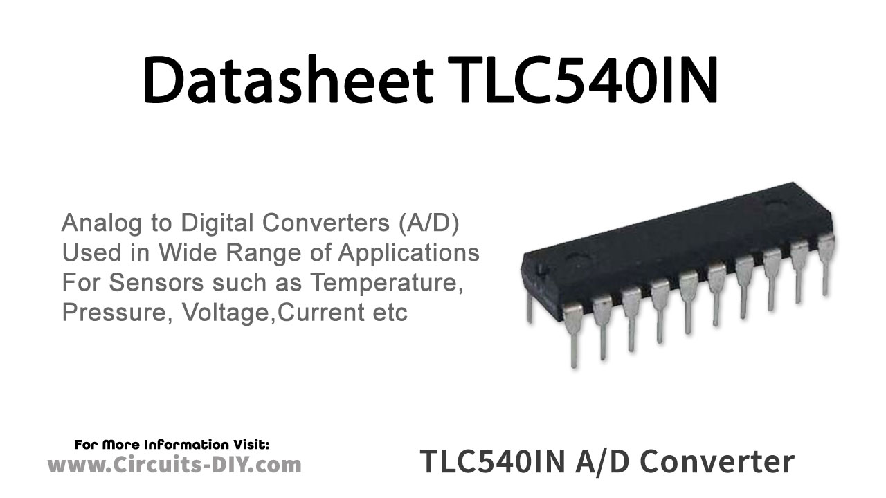
The TLC540IN is CMOS A/D converters built around an 8-bit switched capacitor successive-approximation A/D converters. They are designed for serial interface to a microprocessor or peripheral via a 3-state output with up to four control inputs, including independent SYSTEM CLOCK, I/O CLOCK, chip select (CS), and ADDRESS INPUT. A 4-MHz system clock for the TLC540 and a 2.1-MHz system clock for the TLC541 with a design that includes simultaneous read/write operation allow high-speed data transfers and sample rates of up to 75,180 samples per second for the TLC540 and 40,000 samples per second for the TLC541.

TLC540IN Pinout

TLC540IN Pin Configuration
| Pin No | Pin Name | Description |
|---|---|---|
| 1 | IN A0 | Input Pin A0 |
| 2 | IN A1 | Input Pin A1 |
| 3 | IN A2 | Input Pin A2 |
| 4 | IN A3 | Input Pin A3 |
| 5 | IN A4 | Input Pin A4 |
| 6 | IN A5 | Input Pin A5 |
| 7 | IN A6 | Input Pin A6 |
| 8 | IN A7 | Input Pin A7 |
| 9 | IN A8 | Input Pin A8 |
| 10 | GND | Ground Pin |
| 11 | IN A9 | Input Pin A9 |
| 12 | IN A10 | Input Pin A10 |
| 13 | REF- | Negative Reference Voltage |
| 14 | REF+ | Positive Reference Voltage |
| 15 | CS’ | Chip Select (Active Low) |
| 16 | DATA OUT | Data output Pin |
| 17 | ADDRESS IN | Address Input Pin |
| 18 | I/O CLK | Input /Output Clock Pin |
| 19 | SYS CLK | System Clock Pin |
| 20 | VCC | Supply Voltage |
TLC540IN Features
- 8-Bit Resolution A/D Converter
- Microprocessor Peripheral or Stand-Alone Operation
- On-Chip 12-Channel Analog Multiplexer
- Built-in Self-Test Mode
- Software-Controllable Sample and Hold
- Total Unadjusted Error . . . ±0.5 LSB Max
- TLC540 is capable of higher speed
- Pinout and Control Signals Compatible with TLC1540 Family of 10-Bit A/D Converters
- CMOS Technology
TLC540IN Specification
- Channel Acquisition Sample Time 2 µs
- Conversion Time (Max) 9 µs
- Samples per Second (Max) 75 x 103
- Power Dissipation (Max) 12.5 mW
You can download this datasheet for TLC540IN 8-bit A/D Converter with MUX from the link given below:
Related posts:
 TIP141 NPN Power Darlington Transistor - Datasheet
 CD4029 Binary-Decade Up-Down Counter - Datasheet
 GBPC3510A 1000V 35A Bridge Rectifier - Datasheet
 MJE13006 NPN High Voltage Power Transistor - Datasheet
 IRF9640 11A 200V P-Channel Power MOSFET - Datasheet
 MUR1660CT 8A 600V Dual Ultra-Fast Recovery Diode -Datasheet


