
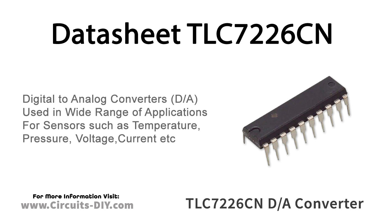
The TLC7226CN is consist of four 8-bit voltage-output digital-to analog converters (DACs) with output buffer amplifiers and interface logic on a single monolithic chip. Separate on-chip latches are provided for each of the four DACs. Data is transferred into one of these data latches through a common 8-bit TTL/CMOS-compatible 5-V input port. Control inputs A0 and A1 determine which DAC is loaded when WR goes low. The control logic is speed compatible with most 8-bit microprocessors. Each DAC includes an output buffer amplifier capable of sourcing up to 5 mA of output current. The TLC7226 performance is specified for input reference voltages from 2 V to VDD − 4 V with dual supplies.
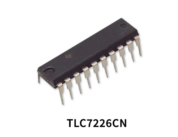
TLC7226CN Pinout
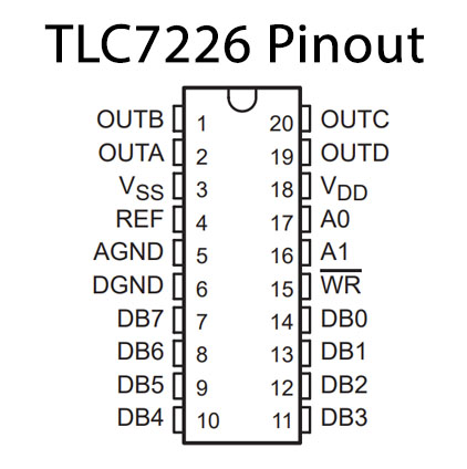
TLC7226 Pin Configuration
| Pin No | Pin Name | Description |
|---|---|---|
| 1 | OUTB | DACB output |
| 2 | OUTA | DACA output |
| 3 | VSS | Negative supply voltage input terminal |
| 4 | REF | Voltage reference input |
| 5 | AGND | Analog Ground |
| 6 | DGND | Digital Ground |
| 7 | DB7 | Digital DAC data input DB7 |
| 8 | DB6 | Digital DAC data input DB6 |
| 9 | DB5 | Digital DAC data input DB5 |
| 10 | DB4 | Digital DAC data input DB4 |
| 11 | DB3 | Digital DAC data input DB3 |
| 12 | DB2 | Digital DAC data input DB2 |
| 13 | DB1 | Digital DAC data input DB1 |
| 14 | DB0 | Digital DAC data input DB0 |
| 15 | WR’ | Write input (Active Low) |
| 16 | A1 | DAC select input A1 |
| 17 | A0 | DAC select input A0 |
| 18 | VDD | Positive supply voltage input terminal |
| 19 | OUTD | DACD output |
| 20 | OUTC | DACC output |
TLC7226CN Features
- Four 8-Bit D/A Converters
- Microprocessor Compatible
- TTL/CMOS Compatible
- Single Supply Operation Possible
- CMOS Technology
Application
- Process Control
- Automatic Test Equipment
- Automatic calibration of large system nd parameters, e.g. Gain/Offset
You can download this datasheet for TLC7226CN Quad 8-bit D/A Converter from the link given below: