Introduction
In this Tutorial, we are going to make a “200-watt MOSFET amplifier circuit class G”. MOSFET is an abbreviation of Metal Oxide Semiconductor Field Effect Transistor. which contains four-terminal ports that include a gate, source, drain, and body. However, because the body of the MOSFET transistor is not considered the port, thus it is a three-terminal device.
Another name for MOSFET is the Insulated Gate Field Effect Transistor (IGFET). MOSFET Transistor is a field-effect transistor with a thin film of silicon oxide between the gate or drain and the channel. Because of its compact size, a MOSFET is specially intended or developed to be easily produced in a microprocessor.
MOSFET is used to make different kinds of amplifiers or to configure different classes of amplifiers. In our previous article, we discussed and made some classes of amplifiers. But, this article is about class G. So, before making a circuit let us briefly discuss Class G.
Class G Amplifier
In some ways, a Class-G amplifier is similar to a series output device amplifier. This configuration is uncommon, although it is occasionally used to increase the safe operating region for the output transistors by restricting the voltage across each transistor pair.
Hardware Required
| S.no | Component | Value | Qty |
|---|---|---|---|
| 1. | Transistor | 2SA872, BC648, 2SD668, BD139, 2SC1775, 2SD669, 2SB649, 2SK176, 2SD551, 2SB681, 2SJ56 | 2,2,4,1, 1,1,1,1, 1,1,1 |
| 2. | Resistor | 470K,2.2K,12K,33K,10K,2.7K, 39K,56Ω,270Ω,200Ω,33Ω,47Ω, 1.8K,1.2K,68K,10K,0.3Ω,150Ω,220Ω, 470Ω,100Ω | 1,1,1,1,1,1, 1,1,1,1,1,1, 2,2,6,2,2,2,2, 2,3 |
| 3. | Ceramic Capacitor | 0.1uF,0.22uF,0.47uF,0.0022uF,1uF, 22pF,4pF,100pF,390pF,1pF,75pF | 1, 1, 2, 2, 2 1, 1, 1, 1, 2, 2 |
| 4. | Electrolyte Capacitor | 100uF, 220uF | 3, 1 |
| 5. | Diode | 1N4148, 1N5403 | 3, 2 |
| 6. | Variable Resistor | 1K | 1 |
| 7. | Speaker | – | 1 |
| 8. | Zener Diode | – | 1 |
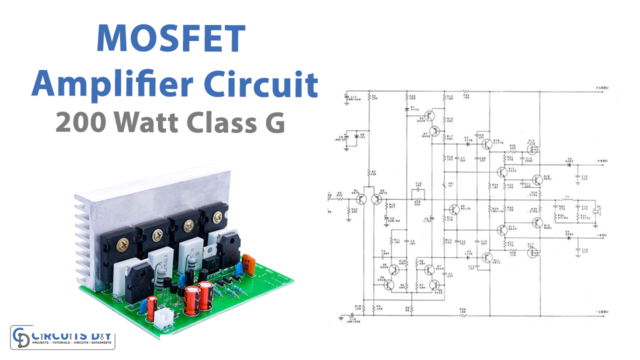
Circuit Diagram

Working Explanation
The input signal is routed through C1 to the base of transistor Q1, which is linked to transistor Q2 as the differential amplifier. This signal is then increased to section 2 which includes Q3 and Q4. The signal then travels to the transistors driver (Q12, Q13) to operate the output transistors Q15, and Q16. Finally, the output signal serves as a driving signal for the speakers.
Both transistors Q14 and Q15 will not operate in the lower signal range. When the peak signal arrives, it will go to D3, D4, and bias Q10 and Q11 to run. As a result, the MOSFETs Q14 and Q17 function properly. This causes power supply 2 to deliver up to 100 volts to the amplifier section.
Application Uses
- Class G design is uncommon. However, it is used to increase the safe operating region for the output transistors