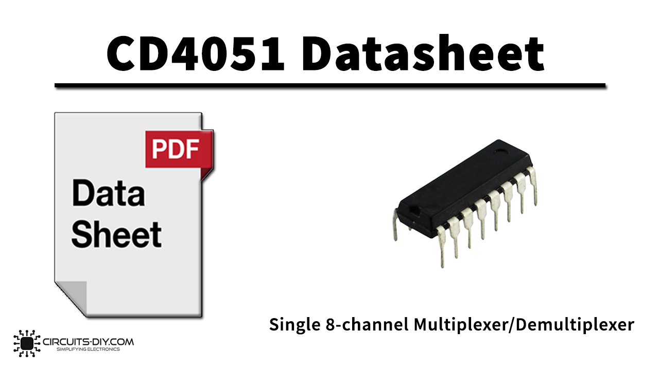
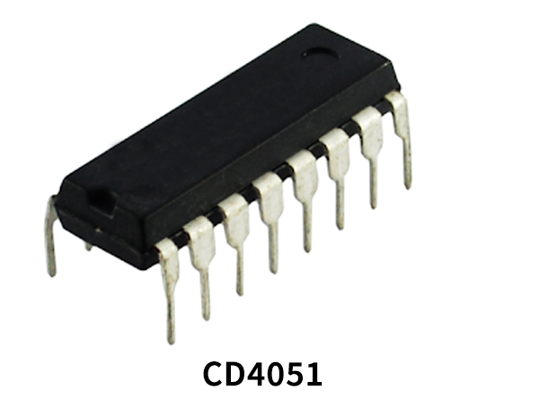
The CD4051 is a part of CD4000 IC series, made by using the complementary MOS (CMOS) technology. CD4051 is a single 8-channel multiplexer having three binary control inputs. A, B, and C, and an inhibit input. The three binary signals select 1 of 8 channels to be turned “ON” and connect the input to the output. The multiplexer circuits dissipate extremely low quiescent power over the full VDD−VSS and VDD−VEE supply voltage ranges, independent of the logic state of the control signals. When a logical “1” is present at the inhibit input terminal all channels are “OFF”. The IC offers a wide array of features such as high noise immunity and low thermal dissipation.
Multiplexer
A multiplexer is a combinational logic circuit that switches one of several input lines to a single common output line. The select lines determine which input is connected to the output, and also to increase the amount of data that can be sent over a network within a certain time. It is also called a data selector.
Demultiplexer
A decoder/demultiplexer is a combinational logic circuit & an integral part of today’s consumer scale electronics. It is designed to switch one common input line to one of several separate output lines. So, A demultiplexer converts a serial data signal at the input to parallel data at its output lines.
CD4051 Key Features
- Wide range of digital and analog signal levels: digital 3 – 15V, analog to 15Vp-p
- Low “ON” resistance: 80Ω (typ.) over entire 15Vp-p signal-input range for VDD − VEE = 15V
- High “OFF” resistance:
- channel leakage of ±10 pA (typ.) at VDD − VEE = 10V
- Logic level conversion for digital addressing signals of
- 3 – 15V (VDD − VSS = 3 – 15V) to switch analog signals
- to 15 Vp-p (VDD − VEE = 15V)
- Matched switch characteristics:
- ∆RON = 5Ω (typ.) for VDD − VEE = 15V
- Very low quiescent power dissipation under all
- digital-control input and supply conditions:
- 1 µ W (typ.) at VDD − VSS = VDD − VEE = 10V
- Binary address decoding on chip
CD4051 Pinout
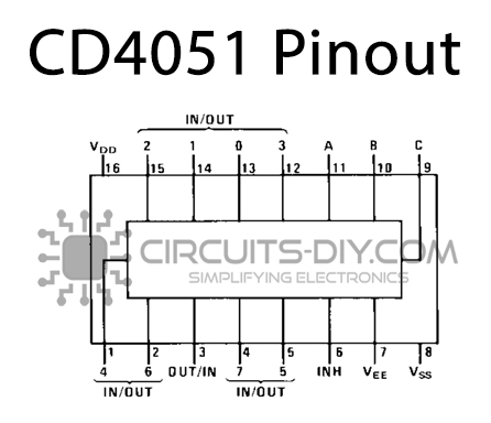
| Pin No | Pin Name | Description |
|---|---|---|
| 1 | I/O 4 | channel 4 i/o |
| 2 | I/O 6 | channel 6 i/o |
| 3 | O/I | common i/o |
| 4 | I/O 7 | channel 7 i/o |
| 5 | I/O 5 | channel 5 i/o |
| 6 | INHIBIT | disable all channel |
| 7 | VEE | Emitter supply |
| 8 | VSS | source supply |
| 9 | C | input c |
| 10 | B | input b |
| 11 | A | input a |
| 12 | I/O 3 | channel 3 i/o |
| 13 | I/O 0 | channel 0 i/o |
| 14 | I/O 1 | channel 1 i/o |
| 15 | I/O 2 | channel 2 i/o |
| 16 | VDD | Drain supply |
Application
- Analog and Digital Multiplexing and Demultiplexing
- A/D and D/A Conversion
- Signal Gating
- Factory Automation
- Televisions
- Appliances
- Consumer Audio
- Programmable Logic Circuits
- Sensors
CD4051 Datasheet
You can download the datasheet for CD4051 Single 8-channel Multiplexer/Demultiplexer from the link given below:
See Also: CD4526 Divide-by-N Counter – Datasheet | CD4527 BCD Rate Multiplier – Datasheet | CD4093 Quad 2-Input NAND Schmitt Trigger – Datasheet