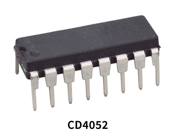
The CD4052 analog multiplexers/demultiplexers are digitally controlled analog switches having a low “ON” impedance and very low “OFF” leakage currents. Control of analog signals up to 15Vp-p can be achieved by digital signal amplitudes of 3−15V. CD4052BC is a differential 4-channel multiplexer having two binary control inputs, A and B, and an inhibit input. The two binary input signals select 1 or 4 pairs of channels to be turned on and connect the differential analog inputs to the differential outputs. The MUX/DEMUX circuits dissipate extremely low quiescent power over the full VDD−VSS and VDD−VEE supply voltage ranges, independent of the logic state of the control signals. The output of the IC always comes in TTL which makes it easy to work with other TTL devices and microcontrollers. The IC also constitutes a wide array of features such as thermal overload protection & ESD protection.
Multiplexer
A multiplexer is a combinational logic circuit that switches one of several input lines to a single common output line. The select lines determine which input is connected to the output, and also to increase the amount of data that can be sent over a network within a certain time. It is also called a data selector.
Demultiplexer
A decoder/demultiplexer is a combinational logic circuit & an integral part of today’s consumer scale electronics. It is designed to switch one common input line to one of several separate output lines. So, A demultiplexer converts a serial data signal at the input to parallel data at its output lines.
CD4052 Key Features
- Wide range of digital and analog signal levels:
- digital 3 – 15V, analog to 15Vp-p
- Low “ON” resistance: 80Ω (typ.) over entire 15Vp-p
- signal-input range for VDD − VEE = 15V
- High “OFF” resistance:
- channel leakage of ±10 pA (typ.) at VDD − VEE = 10V
- Logic level conversion for digital addressing signals of
- 3 – 15V (VDD − VSS = 3 – 15V) to switch analog signals
- to 15 Vp-p (VDD − VEE = 15V)
- Matched switch characteristics:
- ∆RON = 5Ω (typ.) for VDD − VEE = 15V
- Very low quiescent power dissipation under all
- digital-control input and supply conditions:
- 1 µ W (typ.) at VDD − VSS = VDD − VEE = 10V
- Binary address decoding on chip
CD4052 Pinout
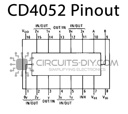
| Pin No | Pin Name | Description |
|---|---|---|
| 1 | Y0 | Channel 0 Input / Output |
| 2 | Y2 | Channel 2 Input / Output |
| 3 | Y | Common Output / Input |
| 4 | Y3 | Channel 3 Input / Output |
| 5 | Y1 | Channel 1 input/output |
| 6 | INH | Enable pin |
| 7 | VEE | Emitter supply |
| 8 | VSS | source supply |
| 9 | B | Channel Selection pin |
| 10 | A | Channel Selection pin |
| 11 | X3 | Channel 3 Input / Output |
| 12 | X0 | Channel 0 Input / Output |
| 13 | X | Common Output / Input |
| 14 | X1 | Channel 1 input/output |
| 15 | X2 | Channel 2 Input / Output |
| 16 | VDD | Drain supply |
Application
- Multiplexer and Demultiplxer circuit
- A/D and D/A converter circuits
- Network switching
- Programmable Logic circuits.
CD4052 Datasheet
You can download the datasheet for CD4052 Differential 4-channel Multiplexer/Demultiplexer IC from the link given below:
See Also: CD4504 Hex Voltage Level Shifter – Datasheet | CD4521 24-Stage Frequency Divider – Datasheet | CD4555 Dual Binary 1 of 4 Decoder – Datasheet