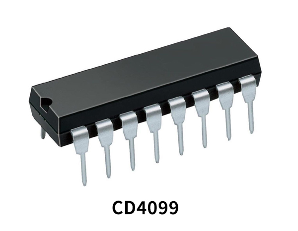
CD4099 IC belongs to the CD4000 IC series. CD4099 is an 8 – bit addressable latch with three address inputs (A0–A2), an active low enable input (E), active high clear input (CL), a data input (D), and eight outputs (Q0–Q7). Data is entered into a particular bit in the latch when that bit is addressed by the address inputs and the enable (E) is LOW. Data entry is inhibited when enabling pin (E) is HIGH. All outputs are LOW when clear pin (CL) and enable pin (E) are HIGH. Channel demultiplexing occurs when clear (CL) is HIGH and enable (E) is LOW. The bit that is addressed has an active HIGH output that follows the data input while all unaddressed bits are held LOW. The IC offers many features such as low thermal dissipation, high noise immunity, and operative flexibility in terms of workability voltages.
What is an Addressable Latch?
An addressable latch is a digital logic circuit that can be used to store a bit of digital information or a digital state. Addressable Latching logic circuits are used to capture, or ‘latch’ the logic level which is present on the Data line when the clock input is high. For example, in a D-type latching circuit, If the data on the D line changes state while the clock pulse is high, then the output, Q, follows the input, D. When the CLK input falls to logic 0, the last state of the D input is trapped and held in the latch.
CD4099 Key Features
- Wide supply voltage range: 3.0V to 15V
- High noise immunity: 0.45 VDD (typ.)
- Low power TTL: fan out of 2 driving 74L
- compatibility: or 1 driving 74LS
- Serial to parallel capability
- Storage register capability
- Random (addressable) data entry
- Active high demultiplexing capability
- Common active high clear
CD4099 Pinout

| Pin No | Pin Name | Description |
|---|---|---|
| 1 | Q7 | Output Pin 7 of Latch |
| 2 | CL | Clear Output Pin |
| 3 | D | Data Input |
| 4 | E’ | Enable Pin |
| 5 | A0 | Input Pin 0 of Latch |
| 6 | A1 | Input Pin 1 of Latch |
| 7 | A2 | Input Pin 2 of Latch |
| 8 | VSS | Source Supply |
| 9 | Q0 | Output Pin 0 of Latch |
| 10 | Q1 | Output Pin 1 of Latch |
| 11 | Q2 | Output Pin 2 of Latch |
| 12 | Q3 | Output Pin 3 of Latch |
| 13 | Q4 | Output Pin 4 of Latch |
| 14 | Q5 | Output Pin 5 of Latch |
| 15 | Q6 | Output Pin 6 of Latch |
| 16 | VDD | Drain Supply |
Application
- Multi-line decoders
- A/D converters
CD4099 Datasheet
You can download the datasheet for CD4099 8-bit Addressable Latch IC from the link given below:
See Also: CD4538 Dual Precision Monostable Multivibrator – Datasheet | CD4541 Oscillator Programmable Timer – Datasheet | CD40110 Decade Up/Down Counter – Datasheet


1 thought on “CD4099 8-bit Addressable Latch – Datasheet”
Comments are closed.