HDI PCB technology is a decisive response to ever changing consumer demand. With HDI technology, designers can incorporate more components on each side of a raw PCB. So, In today’s article, we’ll take a deep dive into the HDI Printed Circuit Board (PCB) Design Benefits and applications and how it has revolutionized the consumer PCBA industry.
Component density on PCB is ever increasing as per Moore’s Law that states ” The number of transistors on a microchip double every two years, though the cost of computers is halved”. With the reducing technology size, it has become imperative to consider the fact that PCB’s with higher component density per square cm are becoming a new need of the industry, especially when it comes to consumer electronics; technology size reduction of smartphones and PCs are a prime example.
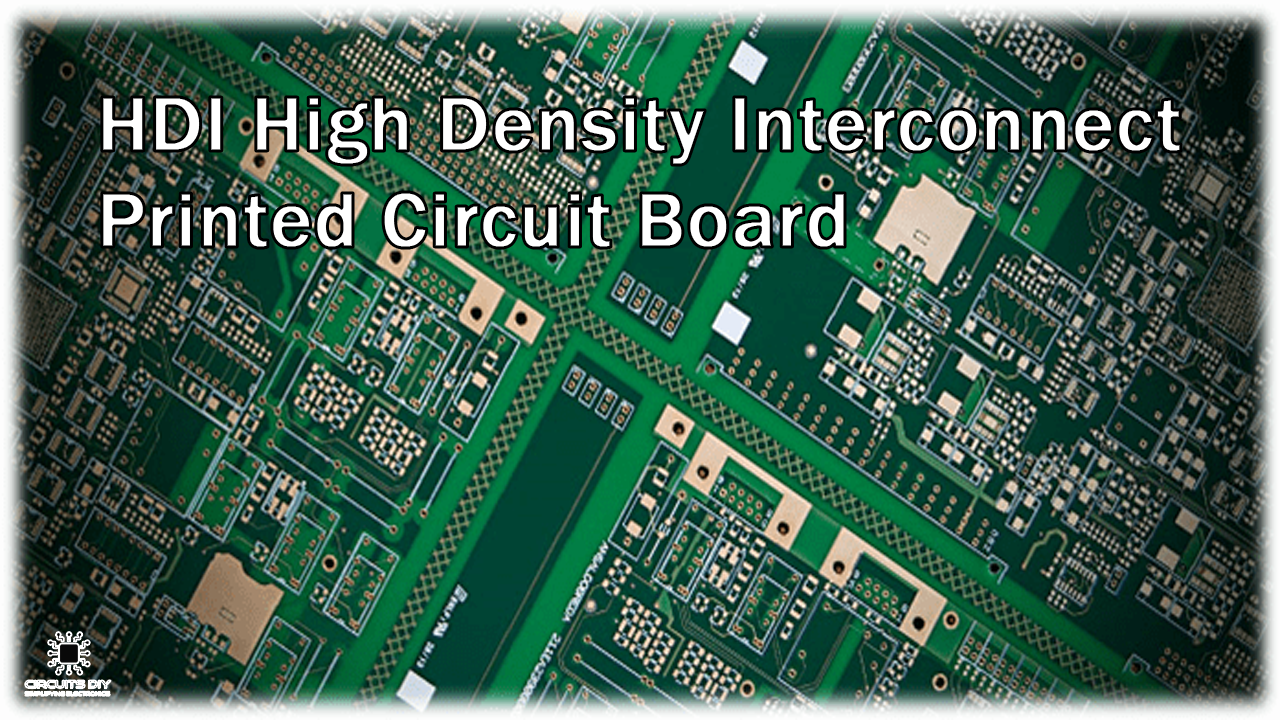
What is an HDI Printed Circuit Board?
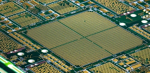
HDI Printed Circuit Board (High Density Interconnect) technology enhances the functionality of conventional PCBs by optimizing space that’s available, by increasing the number of circuits that can be included. Through creating smaller components and placing vias more efficiently, HDI technology frees up real estate on the PCB. So, users can experience improved functionality and data storage.
JLCPCB is the foremost PCB prototype & manufacturing company in china, providing us with the best service we have ever experienced regarding (Quality, Price Service & Time).
Benefits of Using HDI Printed Circuit Boards
1) Minimizes Crossing Delays & Signal Loss
In HDI PCBs, circuit board components are in close position to each other, this causes the signals to travel faster between units, which ultimately reduces crossing delays and minimizes signal loss.

2) Higher Processing Power Within a Small Surface Area
At this point, we all know that HDI PCBs are more interconnected and require a smaller surface area. But the fact is that they’re even more compact than simple PCBs. Yet, they provide the same (and sometimes higher) processing power as a standard PCB.
3) Maintains Signal Integrity & Diminishes Signal Scatter
HDI PCBs also integrate via in pad and blind via technology. This configuration keeps components closer and preserves the integrity of the signal and reduces signal scatter. This promotes the operational health of the PCB. Allowing it to function correctly for a long time.

4) Less Prone To Errors & More Durable
Since HDI PCBs utilize stacked vias, they have effective resistance against variable environmental conditions. This means that the finished product is less prone to errors and is way more durable than a normal PCB.
HDI PCB Applications
The applications of HDI PCBs cover a wide industrial domain. Some of them are provided below:
- Provides efficient and higher density transmission and computation in smaller areas and the creation of smaller end user products such as smartphones, aerospace equipment, military devices, and medical equipment.
- Many medical devices utilize HDI PCB technology since they can fit in small devices like implants, and imaging equipment.
- HDI PCB technology completely dominates the consumer electronics industry. To illustrate, Apple Co. is currently leading the smartphone industry by using a combination of HDI & ELIC PCB technology.
- Also, HDI is used in military devices and other strategic ordnance like missile and defence systems. Since, HDI PCBs are well suited for extreme environment and hazardous conditions. They are ideal for aerospace and military applications.