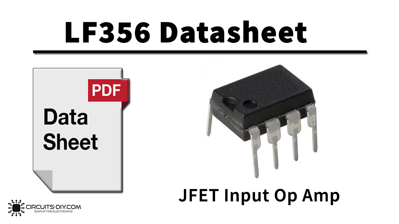
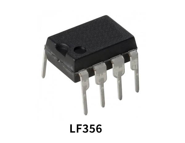
LF356 is a junction field effect transistor input operational amplifier IC. The IC features low input bias and offset currents/low offset voltage and offset voltage drift, coupled with offset adjust which does not degrade drift or common mode rejection. The IC is always available in an 8 – pin hermetically sealed dual in line IC package (DIP). LF356 has a wide range of working conditions, a wide array of operating voltages, and is compatible with almost every TTL, CMOS, & PMOS device. The IC also offers many different features such as high input impedance and high noise immunity.
JFET Operational Amplifier
JFET (Junction field effect transistor) operational amplifier is a simple electronic configuration that boost up a voltage of lower strength to a higher level. Operational amplifier are usually designed to be used with external feedback components such as resistors and capacitors. Operational amplifiers are commonly used in devices such as home theatre systems, VCRs, PCs, Laptops, etc.
LF356 Pinout

LF356 Pin Configuration
| Pin No | Pin Name | Description |
|---|---|---|
| 1 | BALANCE PIN 1 | Offset Balancing Pin 1 |
| 2 | IN 1 | Input Pin 1 |
| 3 | IN 2 | Input Pin 2 |
| 4 | V- | Negative Power Supply |
| 5 | BALANCE PIN 1 | Offset Balancing Pin 2 |
| 6 | OUTPUT | Output Pin |
| 7 | V+ | Positive Power Supply |
| 8 | NC | No Connection |
LF356 Features and Specification
- Low input bias current 30 pA
- Low Input Offset Current 3 pA
- High input impedance 1012X
- Low input offset voltage 1 mV
- small input offset voltage temp. drift 3 mV/§C
- Low input noise current 0.01 pA/0Hz
Application
- Precision high speed integrators
- Fast D/A and A/D converters
- High impedance buffers
- Wideband, low noise, low drift amplifiers
You can download this datasheet for LF356 JFET Input Op Amp from the link given below:
See Also: CD4556 Dual Binary 1 of 4 Decoder Inverter – Datasheet | CD4503 Tri-state Hex Buffer – Datasheet | CD4502 Strobed Hex Inverter/Buffer – Datasheet