Introduction
Solar power generation is widespread these days; therefore, when we think about solar energy, we picture panels arranged on a house’s roof. These panels convert Sun’s light into electricity, which is then sent to various devices throughout the home. It may seem simple, but it involves much more than just a few panels and cost-free electricity for the house. It requires various essential components, including inverters. So, in this tutorial, we will make the “PV Solar Inverter Circuit diagram.”
The inverter’s function is to change the DC output the solar panels have collected into an AC. Please be aware that the various appliances or electronics in your home run on AC, not DC.
Hardware Required
| S.no | Component | Value | Qty |
|---|---|---|---|
| 1. | IC | CD4047 | 1 |
| 2. | Voltage Regulator IC | LM317 | 1 |
| 3. | Diode | 1N4007 | 2 |
| 4. | Schottky Diode | 3A, 50V | 1 |
| 5. | Solar Panel | 12V | 1 |
| 6. | Metal Oxide Varistor MOV | RDN240 | 1 |
| 7. | LED | – | 1 |
| 8. | Reed Switch | – | 1 |
| 9. | MOSFET | IRF540 | 2 |
| 10. | Potentiometer | 2K, 100K | 1, 1 |
| 11. | Capacitor | 0.1uF, 2200uF, 0.01uF, 22uF | 2, 1, 1, 1 |
| 12. | Resistor | 820Ω, 220Ω, 330Ω, 680Ω, 20KΩ | 1, 3, 1, 1, 1 |
| 13. | Transformer | – | 1 |
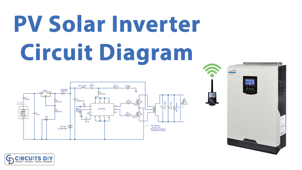
Circuit Diagram
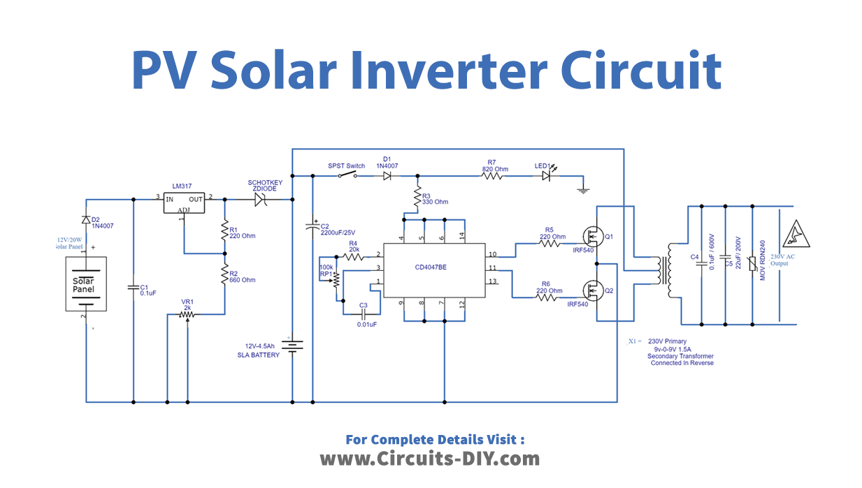
Construction of Circuit
There are five stages of this Circuit:
- PV Solar panel
- Battery Charger
- Switching Pulse Oscillator
- Switching Device
- Step Up transformer
Solar Panel
This PV Solar Inverter Circuit uses a 12-volt/20-watt solar panel to obtain input bias. When exposed to the open Sun, the solar panel produces a peak output of 12 volts at 1600 mA.
Battery Charger
Here, a three-terminal positive voltage regulator with changeable settings named LM317 is utilized, and it has a current rating of more than 1.5A. 12/4.5Ah SLA Battery receives the regulator’s final output, which acts as DC bias for the inverter circuit.
Switching Pulse Oscillator
This switching pulse is produced by the multivibrator IC CD4047, which operates at low power and is offered in a 14-pin dual in-line package. Pins 13 and 11 give a complete oscillation output and a half oscillation at Pins 10 and Q, respectively. Each output pin provides a 50% duty cycle.
Switching Devices using MOSFET Driver
This inverter circuit uses an IRF540 N Channel power Mosfet as a switching driver. It has high working temperature characteristics and provides quick switching.
Step up Transformer
The output stage is the main component of a solar inverter; here, transformer X1 is utilized in reverse and has the following specifications: 230V primary, 9V-0-9V/1.5A secondary winding transformer. Metal oxide varistor (MOV) safeguards connected electronic equipment. The output voltage from the solar panel is immediately supplied into the LM317 positive regulator circuit, which is regulated to produce 12 volts. The battery is wired to this bias by a Schottky diode.
Working Explanation
The CD4047IC integrated Circuit is connected and set up as an astable multivibrator in this solar inverter circuit. When the SPST switch is turned ON, the Circuit begins to oscillate. The secondary winding of the X1 transformer is driven by the output Q and Q’s, which are directly fed into the switching power Mosfet IRF540. Here, the current flow happens for a specific duration but not for a particular period. As a result, the primary winding coil and variable electromagnet-induced EMF produce alternating current output. Following the number of windings and switching frequency, output voltage and frequency vary.
Application and Uses
- Home automation
- Household equipment
- Power generation feilds
- Modern Transportation, etc