
JLCPCB is a professional PCB manufacturer with having an annual production capacity is 200,000 sq.m., with over 8,000 online orders of Printed boards prototyping and a limited quantity of PCB production per day. But, for this, you need to design your structure on EasyEDA software. And, to design this, some steps need to be followed to design printed circuit boards from JLCPCB.
Structure Design on EasyEDA Software
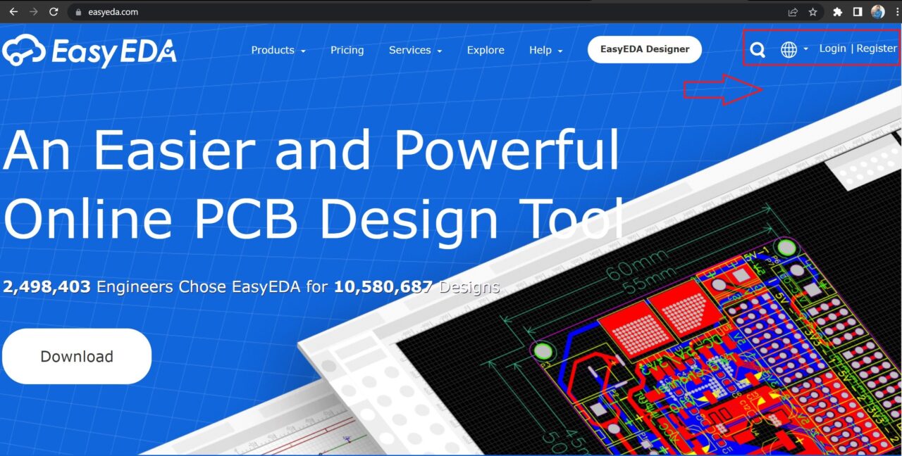
Step one is to structure your design on EasyEDA software, which is a cloud-based PCB designing software. There is no need to install the software, you can also use the web browser. Moreover, this software works on every operating system with access to an updated extensive library that includes thousands of electronic components for circuits and Printed board modeling. It also includes thousand schematic examples. The system is very stable and flexible to learn. The user interface provides a responsive interface. It also can import existing designs done in Eagle, Altium, and KiCad and then edit them on EasyEDA.
Signing Up and Creating New project
Firstly, you need to download and install the software. You can also work online without downloading. The process of installation is simple, you y just need to follow After installation, you need to double click on the EasyEDA icon to open it. Now click the new project and start with New Schematic.

Selection of Components
From the left-hand side, you need to select the components required for your project. For instance, if you want to ground, click on the ground symbol. You can also select ground 1, ground2, ground 3, etc. So, by clicking on that symbol, you can place it on your project wherever you want. Moreover, to search any other component, you have a section search where you can write your required components name to search.

Joining of Components
After the selection of the components, you need to join the components. For this, press W from your keyboard. Now you can join your project components with the help of a wiring tool.
Conversion of Schematic into PCB Layout
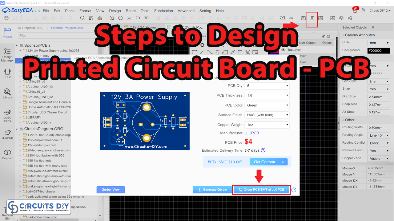
Now you need to convert this schematic into a PCB design layout. And to convert it into PCB design, click on convert project to PCB. You can also view your PCB design layout by pressing on photo view. After that, save the design layout.

Placing Order on JLCPCB
After saving the design layout, you need to send the Gerber file of your board to JLCPCB. Gerber file has all the data related to layers, width spacing, dimensions, and traces of the board. And for sending this, first, you need to open the JLCPCB site and create a free account if you are a new user. After login into your account, go to quote now and upload the Gerber file. After the uploading of Gerber files, you can see all details of your board. Now send the CPL and BOM files. Then select, the elements that you want to use in your board to get from the JLCPCB. make sure to submit all details without errors. Then make a final review of your board design. In the last step complete your order and save it to the cart. Also, select the payment and shipping method.

Related posts:
 Ordering Cheap PCB 2$ PCB Prototype
 Reduce PCB Printing Cost | Top 5 Tips to Cut Cost During PCB Assembly
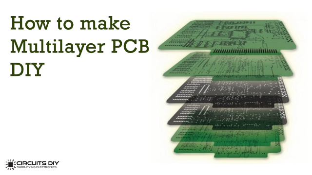 How To Make A Multilayer PCB At Home - A Beginners Guide
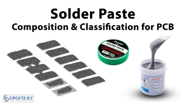 Solder paste Composition and Classification for Printed Circuit Boards
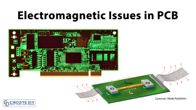 Electromagnetic Issues in PCB
 Single Layer PCB- Application and Advantages


