Contents
hide
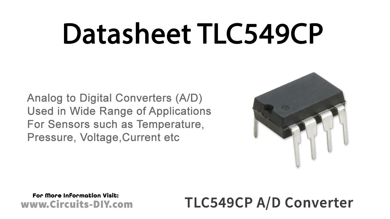
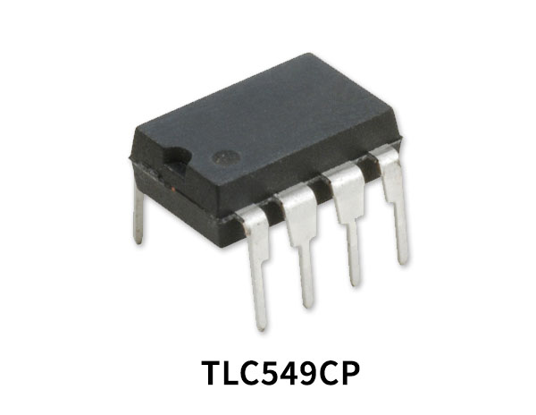
The TLC549CP is CMOS analog-to-digital converter (ADC) integrated circuits built around an 8-bit switched-capacitor successive-approximation ADC. These devices are designed for serial interface with a microprocessor or peripheral through a 3-state data output and an analog input. The TLC548 and TLC549 use only the input/output clock (I/O CLOCK) input along with the chip select (CS) input for data control. The maximum I/O CLOCK input frequency of the TLC548 is 2.048 MHz, and the I/O CLOCK input frequency of the TLC549 is specified up to 1.1MHz.
TLC549CP Pinout
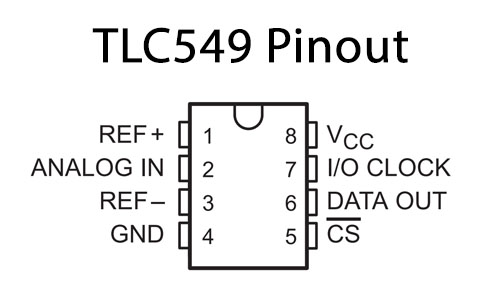
TLC549CP Pin Configuration
| Pin No | Pin Name | Description |
|---|---|---|
| 1 | REF+ | Positive Reference Voltage |
| 2 | ANALOG IN | Analog Input Pin |
| 3 | REF- | Negative Reference Voltage |
| 4 | GND | Ground Pin |
| 5 | CS’ | Chip Select (Active Low) |
| 6 | DATA OUT | Data Output Pin |
| 7 | I/O CLK | Input /Output Clock |
| 8 | VCC | Supply Voltage |
TLC549CP Features
- Microprocessor Peripheral or Stand alone Operation
- 8-Bit Resolution A/D Converter
- Differential Reference Input Voltages
- Conversion Time 17 ms Max
- Total Access and Conversion Cycles Per Second – TLC549 up to 40 000
- On-Chip Software-Controllable Sample-and-Hold Function
- Total Unadjusted Error ±0.5 LSB Max
- 4-MHz Typical Internal System Clock
- Wide Supply Range 3 V to 6 V
- Low Power Consumption 15 mW Max
- Ideal for Cost-Effective, High-Performance
- Pinout and Control Signals Compatible with the TLC540 and TLC545 8-Bit A/D Converters and with the TLC1540 10-Bit A/D Converter
- CMOS Technology
Applications
- Battery-Operated Portable Instrumentation
You can download this datasheet for TLC549CP 8-bit A/D Converter from the link given below: