Introduction
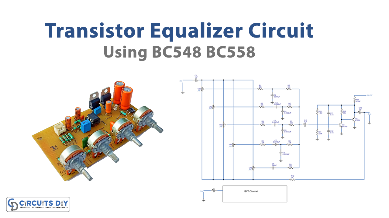
Have you heard about an equalizer circuit? I’m pretty sure, you are, but still, let me give you a simple introduction to a graphic audio equalizer. An equalizer is a circuit that helps to alter a signal by cutting or boosting decibels at specific frequencies. In simpler words, We can adjust the frequency content of an audio stream using an equalizer. Thus, to do a profound analysis, in this Tutorial, we are going to make a “Transistor equalizer circuit diagram”.
To build this circuit, BC548, and BC558 are working as the major components. BC548 is an NPN, while BC558 is a PNP transistor. These are the two different transistor types. The direction of the current is the primary distinction between these two transistors.
NPN transistor activates when current passes through its base. The current in this kind of transistor travels from the collector to the emitter. However, When there is no current flowing through the transistor’s base, a PNP transistor turns ON. The current in this transistor moves from the emitter o the collector. Considering this, it may be said that an NPN transistor turns on by a high signal, whereas a PNP transistor goes on by a low signal.
Hardware Required
| S.no: | Component | Value | QTy |
|---|---|---|---|
| 1. | Transistor | BC548, BC558 | 1, 1 |
| 2. | Resistor | 22K, 33K, 220K, 1.2M, 5.6K, 470 Ohm, 1K | 4, 5, 1, 1, 1, 1, 1 |
| 3. | Capacitor | 1uF, 0.022uF, 0.0047uF, 0.0015uF, 390pF, 0.047uF, 39pF, 100pF | 3, 2, 2, 2, 1, 1, 1, 1 |
| 4. | Variable Resistor | 50K | 5 |
Circuit Diagram
Working Explanation
There are two channels in this Transistor Equalizer Circuit. Let us discuss one channel to understand both. So, here we are discussing the right channel. First, a signal is supplied to the input. Next, capacitor C1 sends a signal to each potentiometer from VR1 to VR5. Here we try to adjust the frequency bands of the potentiometer from lower to higher. For instance, 60 Hz, 100 Hz, 1 kHz, 3 kHz, and 12 kHz respectively for VR1, VR2, VR3, VR4, and VR5. Also, every band contains an Rc network.
Now, the signals coming from each band got combined and become the input for the capacitor C10 which couples to the bases of transistors Q1 and Q2. The higher signal exits a Q1 collector. With the input, it is out of phase. The final output or the highest output signal then comes from Q2’s emitter through C13.
Additionally, certain signals will be sent back to each of the potentiometers through R12.
Application Uses
- To adjust the audio frequency in various types of non-flat audio frequency responses.
- Audio mixer circuit.
- Different alarm and timer circuits, etc.