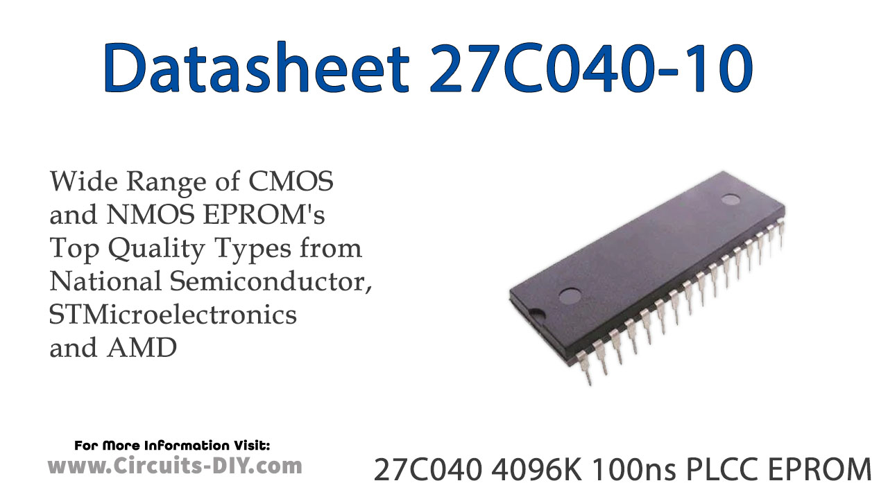
The NM27C040 is a high-performance, 4,194,304-bit Electrically Programmable UV Erasable Read-Only Memory. It is organized as 512K words of 8 bits each. Its pin-compatibility with byte-wide JEDEC EPROMs enables upgrades through 8 Mbit EPROMs. The “Don’t Care” feature on VPP during reading operations allows memory expansions from 1M to 8 Mbits with no printed circuit board changes.
The NM27C040 provides microprocessor-based systems extensive storage capacity for large portions of operating system and application software. Its 120ns access time provides high-speed operation with high-performance CPUs. The NM27C040 offers a single chip solution for the code storage requirements of 100% firmware-based equipment. Frequently used software routines are quickly executed from EPROM storage, greatly enhancing system utility.
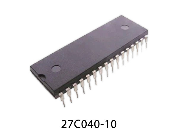
27C040 Pinout

27C040 Pin Configuration
| Pin Number | Pin Name | Description |
|---|---|---|
| 1 | VPP | Programming Supply |
| 2 | A16 | Address Input 16 |
| 3 | A15 | Address Input 15 |
| 4 | A12 | Address Input 12 |
| 5 | A7 | Address Input 7 |
| 6 | A6 | Address Input 6 |
| 7 | A5 | Address Input 5 |
| 8 | A4 | Address Input 4 |
| 9 | A3 | Address Input 3 |
| 10 | A2 | Address Input 2 |
| 11 | A1 | Address Input 1 |
| 12 | A0 | Address Input 0 |
| 13 | O0 | Data Output 0 |
| 14 | O1 | Data Output 1 |
| 15 | O2 | Data Output 2 |
| 16 | VSS | Ground Pin |
| 17 | O3 | Data Output 3 |
| 18 | O4 | Data Output 4 |
| 19 | O5 | Data Output 5 |
| 20 | O6 | Data Output 6 |
| 21 | O7 | Data Output 7 |
| 22 | CE’ | Chip Enable |
| 23 | A10 | Address Input 10 |
| 24 | OE’ | Output Enable |
| 25 | A11 | Address Input 11 |
| 26 | A9 | Address Input 9 |
| 27 | A8 | Address Input 8 |
| 28 | A13 | Address Input 13 |
| 29 | A14 | Address Input 14 |
| 30 | A17 | Address Input 17 |
| 31 | A18 | Address Input 18 |
| 32 | Vcc | Positive Power Supply |
27C040 Key Features
- High performance CMOS
- 120, 150ns access time*
- Simplified upgrade path
- VPP is a “Don’t Care” during normal read operation
- Manufacturer’s identification code
- JEDEC standard pin configuration
- 32-pin PDIP
- 32-pin PLCC
- 32-pin CERDIP
You can download this datasheet for 27C040 4096K 100ns PLCC EPROM – Datasheet from the link given below: