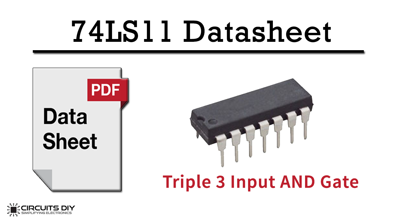
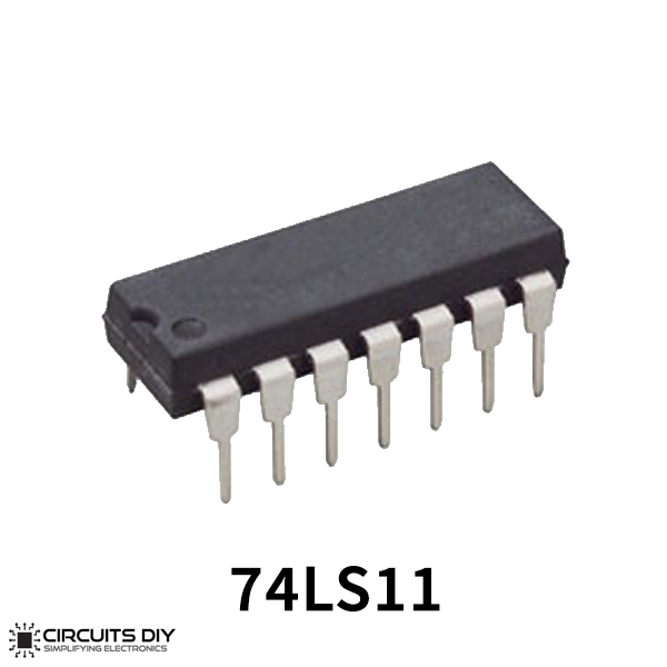
The 74LS11 IC package contains three independent positive logic 3-input AND Gates. It is the part of 74XXYY IC series. The 74LS11 IC has a wide range of working voltage, a wide range of working conditions, and directly interfaces with CMOS, NMOS, and TTL. The output of the IC always comes in TTL which makes it easy to work with other TTL devices and microcontrollers. The IC 74LS11 is smaller in size and it has a much faster speed which makes it reliable in every kind of device.
What is an AND Gate?
An AND Gate is a logical operator/circuit that gives a logical high (1) output only when all of its inputs are high (1), otherwise, it results in a logical low (0). The logic or Boolean expression for a digital logic AND gate is that for Logical Multiplication which is denoted by a single dot or full stop symbol ( . ).
74LS11 Pinout
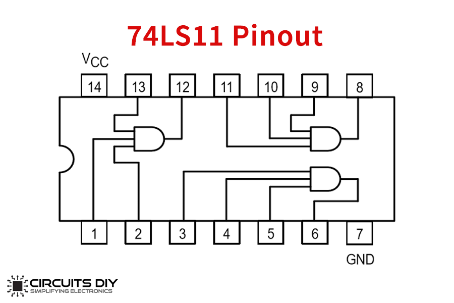
74LS11 Pin Configuration
| Pin No | Pin Name | Description |
|---|---|---|
| 1 | A1 | INPUT 1 of GATE 1 |
| 2 | B1 | INPUT 2 of GATE 1 |
| 3 | A2 | INPUT 1 of GATE 2 |
| 4 | B2 | INPUT 2 of GATE 2 |
| 5 | C2 | INPUT 3 of GATE 2 |
| 6 | Y2 | OUTPUT of GATE 2 |
| 7 | GND | Ground |
| 8 | Y3 | OUTPUT of GATE 3 |
| 9 | A3 | INPUT 1 of GATE 3 |
| 10 | B3 | INPUT 2 of GATE 3 |
| 11 | C3 | INPUT 3 of GATE 3 |
| 12 | Y1 | OUTPUT of GATE 1 |
| 13 | C1 | INPUT 3 of GATE 1 |
| 14 | VCC | Supply Voltage |
74LS11 Specifications
- Supply Voltage 7V
- Input Voltage 7V
- Operating Free Air Temperature Range 0°C to +70°C
- Storage Temperature Range -65°C to +150°C
- Maximum current allowed to draw through each gate output: 8mA
- TTL outputs
- Low power consumption
- Typical Rise Time: 18ns
- Typical Fall Time: 18ns
Applications
- The chip provides TTL outputs that are needed in some systems.
- 74011 IC is usually used in a place where 3 – input logical AND operation is required.
- Also used in devices such as PCs and notebooks.
You can download this Datasheet 74LS11 3-Input AND gate from the link given below:
See Also: 74LS00 Quad Two Input NAND Gate | 7407 Hex Buffer IC | 7404 NOT Gate IC