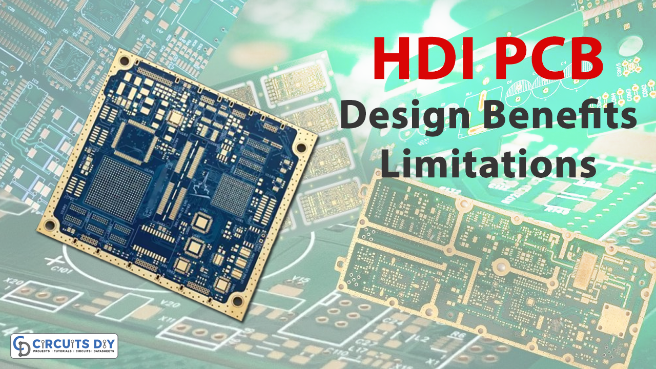
Introduction to HDI-PCB
As the world is evolving, technology is also evolving with it, and humans trying to make things smaller and more reliable. HDI PCB is High-Density Interconnect an emerging technology in PCB where the components are compressed in a tiny space. This board comprises blind and buried his which have a very smaller diameter of about 0.06 or less. The board can transmit high frequency, it has high speed, and the size is small having high-performance material.
JLCPCB is the foremost PCB prototype & manufacturing company in china, providing us with the best service we have ever experienced regarding (Quality, Price Service & Time).

Types of HDI Boards

HDI board has six different types which are given below:
- through vias from the surface to surface
- With buried vias and through vias
- Two or more HDI layers with through vias
- The passive substrate with no electrical connection
- Coreless construction using layer pairs
- Alternate constructions of coreless construction using layer pair
HDI PCB Board Material
The particular material for HDI is Resin Coated Copper (RCC). There are three different kinds of RCC, pure polyimide film, cast polyimide film, and polyimide metalized film. The RCC has very lightweight and it reduced flammability, it has exceptional stability. It promotes the manufacturing of PCB products from surface mount technology to chip-scale packaging, the mechanical drilling is replaced by laser drilling.
RCC was specifically advanced to aid with poor hole quality. It contains ultra-thin copper foil that is attached with tiny nodules. It is suggested to preheat the material for the lamination process of HDI PCB boards. This preheating of the material allows for to vent temperature of the f laminated product.
HDI PCB Design Tips
- For ground connections, use the outer layer while the inner layer will be used to adjust the power plane and vias for routing
- For many layers of HDI, stacking the micro via, ie is more efficient and provides more flexibility
HDI Board Benefits
- Smaller Size: To reduce the number of layers HDI PCB is the best choice. It has vias that are not visible to the naked eye. Due to the smaller size products are more durable and efficient
- Lower Heat transfer: Because of the smaller size, it is difficult for the heat to travel. This also extends the life of PCB and makes it more reliable
- Less Transmission Time: Components are placed very close to each other, and this transmission rate from component to component gets reduced, this decreased the transmission time and increased the signal strength
- Higher Density Transmission: It allows to transmit of higher density in smaller areas which makes it more efficient
- Less Power Usage: It uses less battery power and hence increased the battery life
- Greater number of Components: HDI PCB can incorporate a higher number of components on both sides of the board
Limitations of HDI Boards
- It is still in the evolving state
- It requires more expensive equipment
- It has a lower yield
The Future Of HDI PCB Board
The HDI boards are still in the progressing procedure, it is evolving and technology is emerging day by day. The HDI board can take technology to the next level, and it’s playing an important role in new electronic device creation. The world is running fast and technology is evolving every sing day in this period, so, It’s the technology for the present era that works efficiently with less time and more speed. The technology seems so promising and its demand is increasing every day.
Related posts:
 HQDFM Free Online Gerber Viewer - NextPCB
 Printed Circuit Boards Assembly Overview- Steps and Process
 10+ Best Free PCB Design Software
 Beginners Guide To PCB Routing: Tips & Best Practices
 SMD Components | Commonly Used SMD Parts And Their Identification
 Top 5 Best PCB Electronics Projects For Complete Beginners


