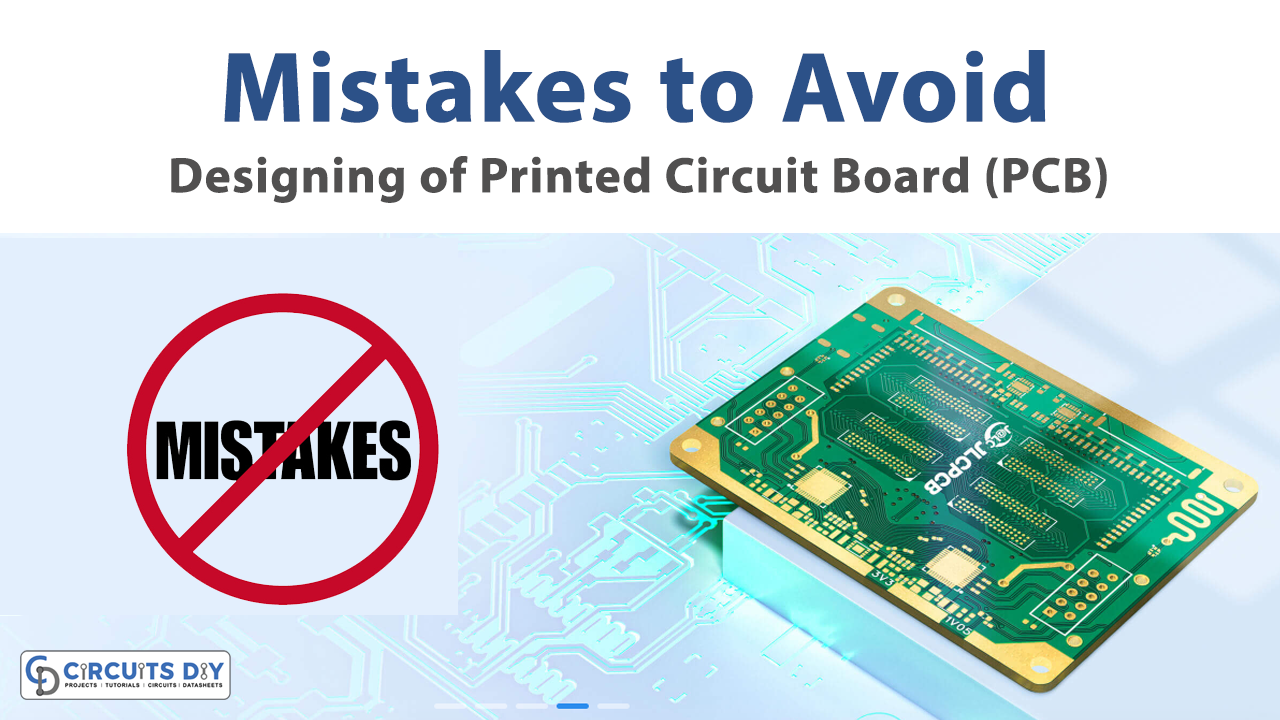
A printed circuit board is the central board in any electronic product. If the design is not adequate, it may damage the device. The poor quality design means, poor quality of PCB and so does the electronic device. The poor quality design harms not only the device but also challenges the reliability of the Printed Board. And, thus in those cases, the durability rate also gets questioned. Therefore, in this article, we will discuss the mistakes to avoid while designing the printed circuit board.
Incorrect Design Tool
The right tool is the basic important and necessary step for an outstanding PCB design. It’s always significant to prefer the tool that suits the requirement of your PCB. Because an inefficient tool can create design delays and may also increase the manufacturing cost. There are several good EDA (Electronic Design Automation) software. So, choose carefully and decide the tool that best satisfies your Printed board.
Inadequate Design Layout
Most of the problems that occur in the printed boards are because of their design. The design includes its circuit diagram and routing. Routing plays a major role and affects the working of any device. If we do not do it properly, the routing may badly affect the board. Routing means the placement of vias that connects the components. If the route traces are not properly placed with length, width, and spaces, it may offer the hope problem in the future. Therefore, it should be done effectively.
Inaccurate position of the decoupling capacitors
We require decoupling capacitors on the Printed circuit board power supply lines. To ensure a stable power supply free from oscillations. It is actually necessary that we always connect these capacitors in parallel with the power supply and placed them as close as possible to the pins of the components that need power. We must properly route the power line coming from the power source on the PCB, in order to get to the decoupling capacitor before going to the pin that needs a stable voltage.
Landing pattern Errors
Landing patterns deal with the size of the pads and, each element or component. And hence their area should always be slightly larger than that of the corresponding footprint. Even a half-millimeter error in measuring pad-to-pad spacing can result inevitably in soldering during the manufacturing process. It may also be misalignments between the printed circuit boards and the electronic components. Good PCB software tools come with an extensive collection of libraries that comprise both the schematic symbol and the landing pattern for each component. If a component is not comprised in these libraries, it is then necessary to add by hand, both the landing pattern and electrical symbol.
Incomplete Revision of the Design
In the PCB designing process, design review is indeed one of the most important elements which should not be underestimated at all. The reviews of the design allow us to verify the project, the functions entrusted to the Printed circuit board, and the interconnections between the different circuits. This also supports designers to avoid the most common design faults.

