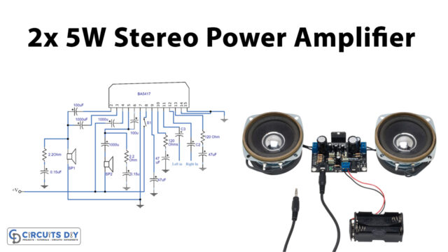
Introduction
In this Tutorial, we are going to make a “TDA2822 stereo amplifier circuit with PCB & datasheet”. A dual low-power audio amplifier called the TDA2822 is housed in an 8-Pin plastic dual in-line box. Having Low crossover distortion, a low quiescent current, and a supply voltage range of 3V to 15V are just a few of the qualities that this IC has to offer. It has two Op-Amps, which are typically used for audio amplification due to their broad bandwidth gain. And, 250 milliwatts of output power can be delivered by the two outputs.
Features of TDA2822
- Low noise and low distortion circuitry
- Small Size (8-pin dip package)
- Only a few external components required
- Contains dual low voltage power amplifies (Built for Stereo Amplification)
- Can also be used in BTL mode
- Low-cost and reliable
TDA2822 Specifications
- Supply Voltage: 3-15V
- Output Power: 3.2 W
- Audio – Load Impedance: 8 Ohms
- Gain: 39 dB
- Operating Supply Current: 12 mA
- Ib – Input Bias Current: 0.1 uA
- PSRR – Power Supply Rejection Ratio: 40 dB
Pin Configuration of TDA2822 IC
| Pin Number | Pin Name |
| 1, 3 | Output |
| 5, 8 | IN- |
| 6, 7 | IN+ |
| 4 | Vcc- |
| 2 | Vcc+ |
Pins Description
- Output: Provides the amplified audio
- IN-: Inverting input, normally remain grounded
- IN+: Noninverting input, where the audio signal is given
- Vcc-: Needs to connect to the negative supply
- Vcc+: Needs to connect with positive supply rail

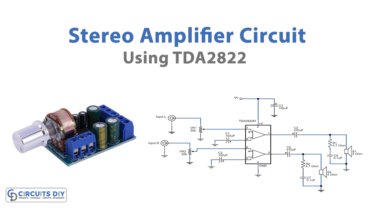
TDA2822 Stereo Amplifier Circuit
Since we have briefly discussed the TDA2822, now let’s make a simple Stereo Amplifier Circuit using this IC.
Hardware Required
| S.no | Component | Value | Qty |
|---|---|---|---|
| 1. | IC | TDA2822 | 1 |
| 2. | Resistor | 4.7 ohms | 2 |
| 3. | Capacitor | 100uf, 470uf, 0.1uf | 3, 2, 2 |
| 4. | Speaker | 4 ohms | 2 |
| 5. | Variable Resistor | 50K | 2 |
Circuit Diagram
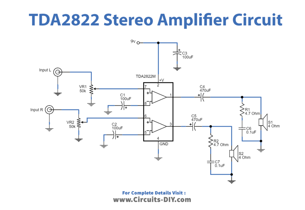
Working Explanation
First, the circuit receives 9V from the power supply. Furthermore, capacitor C3 acts as a filter capacitor to maintain a more constant voltage, when the sound is too erratic. Then, pin 2 of IC1 is a Vcc pin and therefore receives a steady voltage. Additionally, a negative voltage is connected to the circuit’s GND. Both the left and right input signals flow through potentiometers VR1 and VR2. Hence can adjust the music’s volume. capacitors C1 and C2 are there to suppress DC voltage. The signal then successively flows to inputs pins 7, 8, and pin 6. The circuit within the IC operates and increases the audio’s power. Output is coming from pins 1 and 3
Application of TDA2822
- Audio systems
- Preamplifiers
- Headphone amplifiers
- Mini hearing aid devices
- Music players
- Toys
- Cassette players
- Radios, etc