Usually, Being Engineers, we tend to pay most attention to circuit components, and code, but sometimes a critical component of electronics, the PCB layout, remains in neglect. Poor PCB design can cause function and reliability problems. If this is your first-time performing PCB designing, then seeing a chaotic looking rats nest might be a little intimidating. PCB designing is a process in which even the most common mistakes are bound to occur. What are those mistakes? How do we avoid them?. Today, In this article, we will go over the Top 5 PCB Design Tricks And Best practices that will enable you to achieve the level of design perfection you so desire.
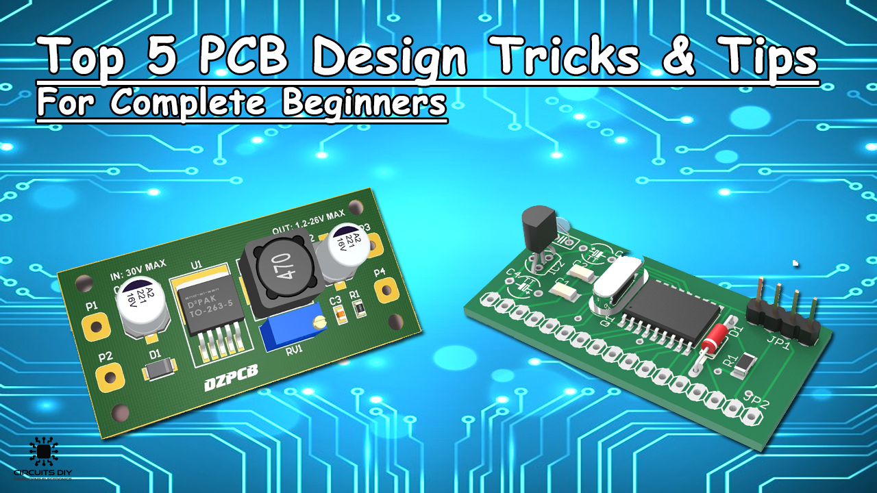
Top 5 PCB Design Tricks And Tips For Beginners
1) 45° Trace Angles Are the Best
Designing with angles greater than 90 degrees can enable acid traps which can be harmful to the circuit board. Utilizing 45-degree angles are better practice as they have a smaller impact on the width of the trace. Narrow angles can cause electromagnetic radiation and copper migration over time and should be avoided.

2) Choose The Right Design Tool
Perhaps the most important step in proper PCB design is to choose a design software that caters to all your design needs. The tool that you use to design your boards should at least minimally meet the essential feature requirements present for your design. I must recommend using easyEDA it’s really simple and easy to use as its name implies.
3) Keep Final Housing In Mind While Designing
Always keep the housing of the final product in mind when designing. Often, when we design PCBs we have no housing decided. But at the end of the day, the PCB needs to be in proper housing. So keep mounting holes there, and choose some readily available and simple housing and design the PCB around that. It is possible that later-on the same housing gets approved and the re-designing is avoided.
4) Keep Sufficient Width Between High Power Traces
The minimum PCB trace width threshold won’t be sufficient if the PCB Board traces has to house currents greater than 500mA. A trace on an outer layer can carry more than an internal trace for the same thickness. This is because the external trace has superior airflow and thermal dissipation. The width depends on how much copper is being used for that layer. Most PCB manufacturers allow you to choose from various copper weights from 0.5 oz/sq.ft to 2.5 oz/sq.ft.
5) Always Perform An End Of the Design Visual Inspection
Perform a thorough visual inspection of the PCB at the end of the design process. This will help you in determining defects such as overlapped traces, faulty pads & vias, design discrepancies, missing & bulging components.
In Conclusion, By following the above Top 5 PCB design tricks you can take your PCB Designing skills to the next level.