Introduction
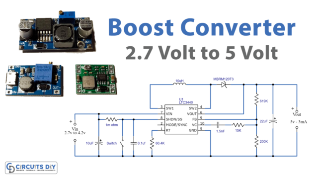
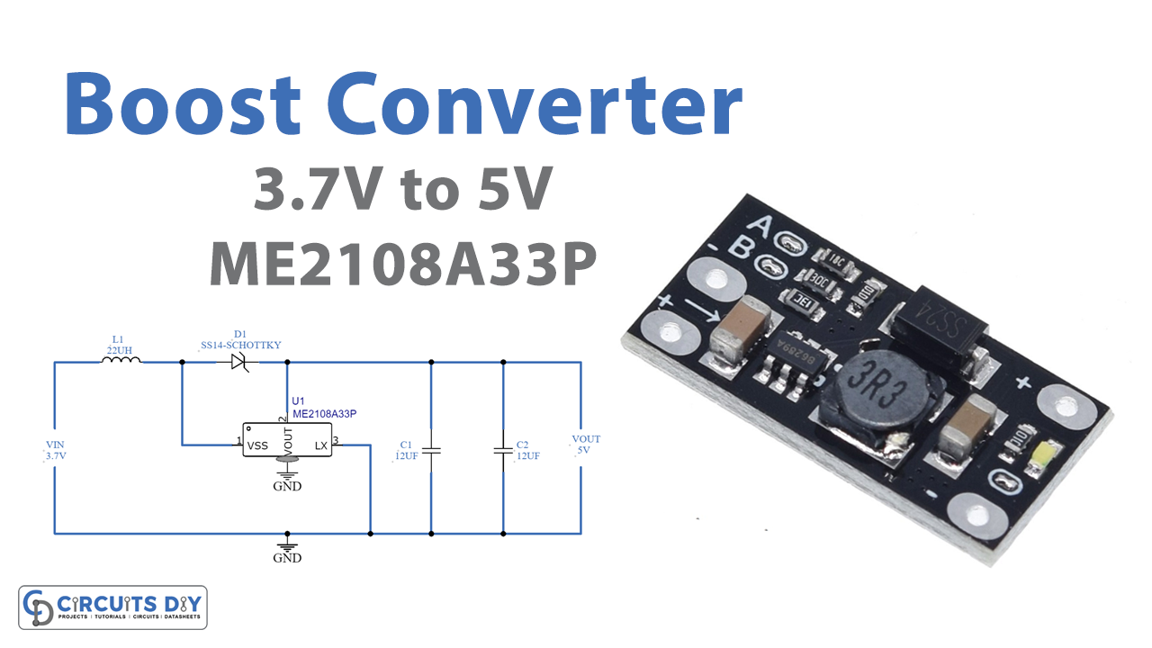
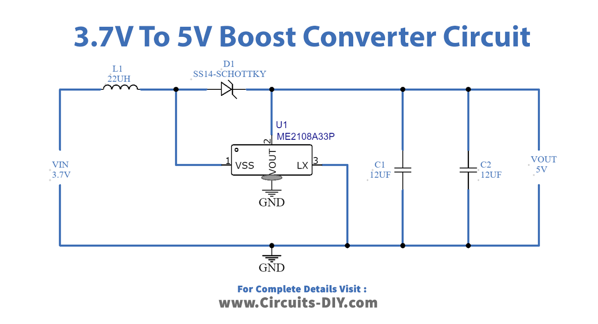
Sometimes while making the circuits, we get in a difficult situation where we want some more supply than the power supply available. For example, we only have 3V DC available but we need 9V or 12 V DC. At this time, the circuit known as the “boost converter” gets utilized. It helps to boost up the input DC voltage and provide it at the output side so that it may get used by the other device that needed the greater voltage. In this tutorial, we are going to “3.7V to 5V Boost Converter”.
Conversion from lower to higher voltage is not that much difficult as we have already learned about the AC to DC converter. But, this circuit is about DC to DC conversion. To increase the input voltage at the output load, the circuit commonly known as voltage booster is used. As the name implies, it takes the input voltage and with the help of some components transforms that voltage into high voltage. The circuit can be made using different methods like inductors, capacitors, semiconductor switches, etc. But, for efficient output, some voltage regulator ICs are also available in the electronic market. Hence, we will use one of them in our project. With the IC ME2108A33P, this circuit also uses the Schottky diode SS14.
Overview of ME2108A33P
Basically, this IC ME2108 is a step-up DC to DC converter IC with a low supply current. This IC lessens the high-frequency switching noise. The output of this boost converter IC can be programmed from 2V to 7V. The IC has three pins and that’s why It requires only three external components to work as a step-up converter. This IC can be used with a low supply current.
Features of Schottky diode SS14
- This diode has the maximum Forward Current of 1Amp.
- The maximum forward voltage at 1Amp is 0.5V.
- The reverse current is 0.5mA.
- The diode has the maximum DC blockage voltage of 40V
Hardware Required
| S.no | Component | Value | Qty |
|---|---|---|---|
| 1. | Regulator IC | ME2108A33P | 1 |
| 2. | Inductor | 22µH | 1 |
| 3. | Schottky diode | SS14 | 1 |
| 4. | Capacitors | 12µF | 2 |
Circuit Diagram
Working Explanation
In this circuit of 3.7V to 5V Boost Converter, the major component is ME2108A33P IC. The internal structure of this IC is so promising and that’s why it requires very few components for its external circuitry. The IC has three pins. It uses a maximum switching frequency of 180KHz. This IC can deliver 400mA output current if the input voltage is 3.0V and the output voltage is fixed at 5.0V. On the input side, we have connected the inductor. By changing the value of the Inductor and output capacitor you can adjust the output voltage range. The Schottky diode SS14 is also wired at the input side, usually used to prevent the circuit from reverse polarity. At the output, capacitors are there to observe the readings.
Code Explanation
Application and Uses
- Telecommunication devices can use this circuit.
- Consumer electronic devices widely use boost converters.
- In battery power supplies, etc.
- Different electronic devices use this circuit.