Introduction
Sometimes while making the circuits, we get into the troublesome situation where we want some more supply than the power supply available. For example, we only have 3V DC available but we need 9V or 12 V DC. At this time, the circuit known as the “boost converter” gets utilized. It helps to boost up the input DC voltage and provide it at the output side so that it may get used by the other device that needed the greater voltage. Conversion from lower to higher voltage is not that much difficult as we have already learned about the AC to DC converter. But, this circuit is about DC to DC conversion. Hence, in this tutorial, we are going to “Boost Converter Circuit 555”
Hardware Required
| S.no | Component | Value | Qty |
|---|---|---|---|
| 1. | IC | NE555 Timer | 1 |
| 2. | NPN Transistor | BC547 | 1 |
| 3. | Diode | 1N4007 | 1 |
| 4. | Potentiometer | 20K | 1 |
| 5. | Inductor | 80µH | 1 |
| 6. | Capacitors | 470pF, 0.01µF, 0.1µF | 1, 1, 1 |
| 7. | Resistor | 1K, 330Ω | 1, 1 |
| 8. | Battery | 3V | 1 |
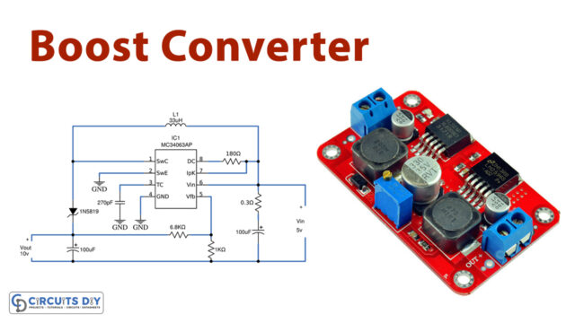
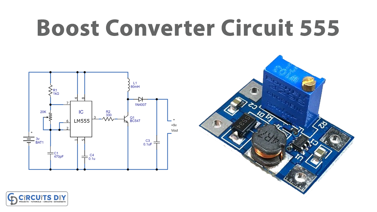
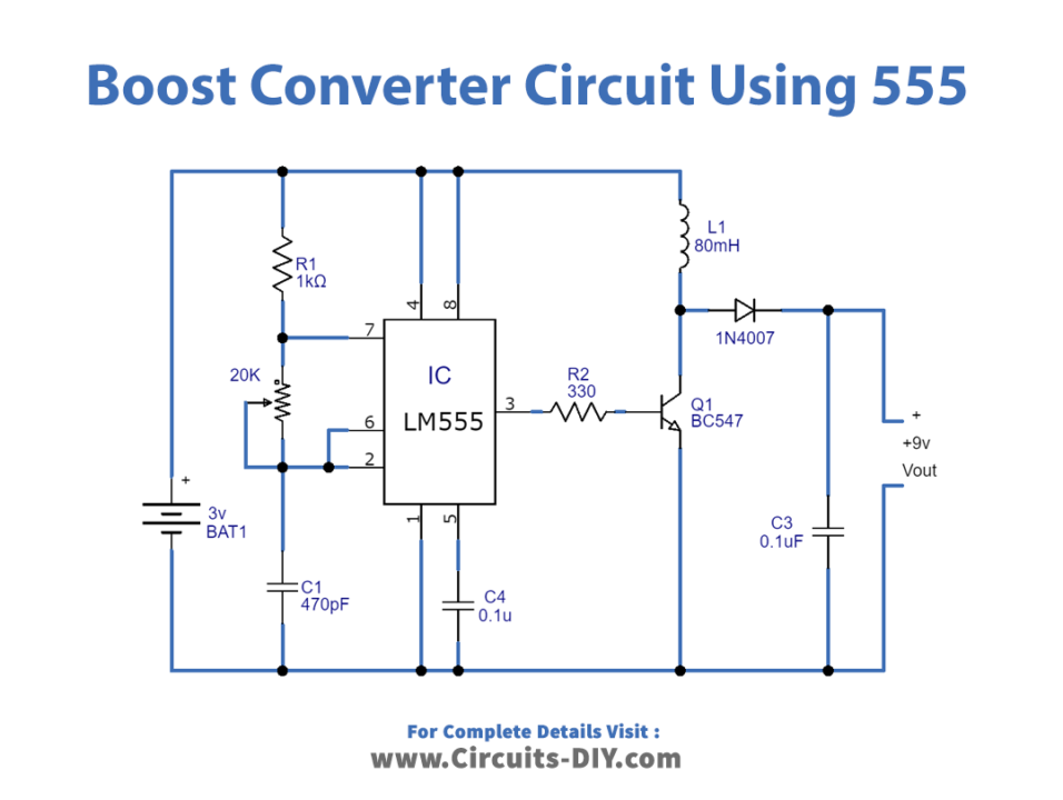
Circuit Diagram
Working Explanation
In this simple Boost Converter Circuit, the 555 timer IC is configured as the astable multivibrator mode. When the 3V supply is given to the IC, it generates a continuous pulse. The pulse frequency can be increased or decreased by a potentiometer wired with the IC. The output of the 555 timer IC has connected to the base of the transistor. This output turns ON the transistor. Transistor performs the amplification. This amplified output is taken at the collector pin of the transistor. Output capacitor C3 removes the ripples.
Application and Uses
- It can be used in photovoltaic cells.
- In battery power supplies, etc.