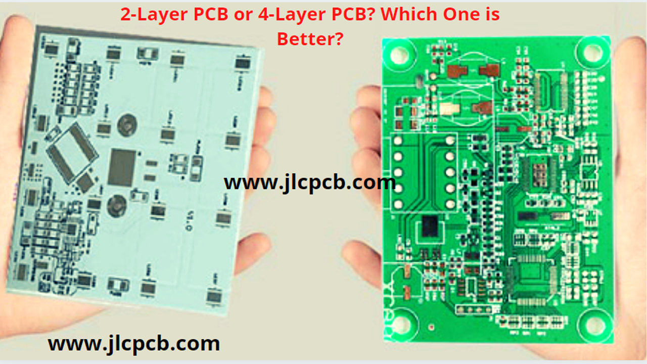
Difference between 2 layer PCB and 4 layer PCB

As the title suggests, you could probably anticipate what the major differences among those two types of PCBs are. Multi-layer PCBs feature numerous layers, whereas double-layer boards have only one layer of core materials, widely known as a substrate. When we take a deeper look at the three main types of PCB boards, we will notice that they have a lot of distinctions in terms of how that is built and also how they work.
The fundamental distinction between a double layer and a multilayer boards design is in the layers stack-up design. The following have been some of the things to think about when putting together your board’s layers stack-up:
- Effectiveness: The operational environment of a finished board, as well as the speed at which the circuits would function, might influence the components used to construct the board. There are more innovative substances than FR-4 that may be best suited for your applications according to your requirements, however, these substances may have an impact on characteristics like impedance calculations. Your PCB product’s assistance would be a significant supply of knowledge in this case.
- Cost: The manufacturing components, and the number of layers, and their layout, would have a significant impact on the board’s end price. You’ll need to consult with your manufacturers to weigh all of your choices.
- Density: While establishing the design of your board’s layers stack up, an additional aspect to consider is the route concentration of your boards. Whenever you have to go around and apply layers to a board’s concept when you’ve already begun your design, it’s excruciating. So may just have to create a variety of adjustments to your designs in addition to reconfiguring your CAD databases. However, if you begin with far too many levels, they would end up spending more for boards than necessary.
- Circuits: In way to construct the best layer layout, you must also consider the needs of the circuit board. Sensitivity transmissions, for example, may require a stripline layers design for optimal operation, which would necessitate the installation of extra grounded surfaces. Different grounding planes would be required for analog and digital circuits, as well as separation for onboard power supply. Everything could get an impact on layer arrangement, which should be considered before beginning the layout.
It’s essential to start arranging and arranging the boards after you’ve collected the information and built your board’s layers stack up within design databases.
Double-Sided PCBs
A double-layer or double-sided board, that has greater layers than a single-layered board but less than a multi-layer board could also be used. Such as single-sided PCBs, double-sided PCBs only have one substrate layer. Those who are distinguished by the presence of a semiconducting metal layer on both ends of the material.
One among 2 ways is used to link circuitry and parts on one part of the boards to many on the other:
- Hole-in-the-Wall: Through-holes are tiny slots carved into the boards via which cables, known as leads, were passed and soldered to the appropriate components.
- Surface Attachments: Those PCBs have leads that are soldered to the boards individually. The boards serve as the product’s cabling surfaces, allowing the circuitry to occupy up minimal area.
The Double-Sided PCB’s Layout and Elements
The sort of double-sided PCB materials used depends on the application. Many circuits boards, nevertheless, have nearly the same core materials. The construction of the PCB, on the other hand, differs from one kind to the next.
The most significant substance composed of fiberglass is the substrates. We could think of it as the PCB’s structure.
- Copper Covering: This might be in the form of a foil or a full copper coating. As a result, it is dependent on the type of boards. If you are using foil or copper covering, the outcome will be the same. A conducting copper coating is included on both sides of double-sided circuit boards.
- A soldering masking is a polymer protection covering. As a result, it avoids short-circuiting of copper. We could think of it as the circuit boards covering. Soldering double-sided PCBs is a crucial stage for long-term reliability.
- Silkscreen seems to be the final step in the silkscreen process. Even though it plays no part in the circuit board’s performance. It is used by producers to display replacement parts. For experimental purposes, item identification was crucial. In addition, users could use text to create their corporate logos or even other data.
Advantages of Double-sided circuits boards
- High-quality: The development and designing of this PCB require a significant amount of effort. As an outcome, high-quality circuit boards are produced.
- Parts Have Enough Room: It has more space for elements. Since the layer is conducting on both ends.
- It contains conducting layer on both ends, giving you more designing options. On both edges, users could connect various electronic parts. As a result, you have a wider range of design alternatives.
- Sinking and Sources Current: You could use it for sink and sources current when utilizing it as a base surface.
- It can be used for a variety of purposes due to its effectiveness.
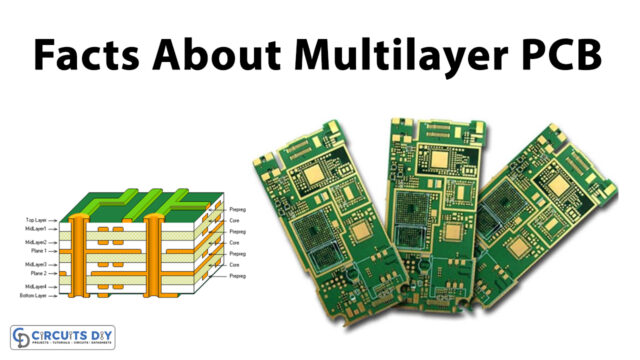
Multi-layer PCBs
3 or even more double-sided boards were placed on top of one another to create multi-layer PCBs. These could potentially hold quite so many boards as you needed, but the biggest one has ever produced has 129 layers. These usually have an even number of layers, ranging from 4 to twelve; uneven numbers might result in post-soldering issues like warping and twisting.
In a multi-layer board, each substrates layers has a conducting material on both ends. The boards were glued together with specific adhesives, and each board is separated by an isolating substance. Solder mask could be found on the multi-layer board’s very outside borders.
Vias enable the various layers to communicate with one another. Those pathways are divided into three categories:
- Through-Hole: Work your way through all of the panel’s layers.
- Attach an exterior layer to an internal layer if you’re blind.
- Entombed: Join two inner surfaces to make them invisible to the outside world.
Multi-layer PCBs are commonly seen in more complicated systems with a large variety of connectors.
The Multi-layer PCBs Layout and Elements
Multi-layer printed circuit boards (PCBs) start to appear more popular as technological advances. The usage of numerous layers on circuit boards is necessitated by the extensive functioning and reduced size of many of today’s electronic gadgets. Multi-layer circuits are used in a variety of devices across sectors, particularly those with several operations and more complicated features.
- Many computing systems, such as motherboard and processors, use multi-layer printed circuits boards. Those boards are included in a wide range of electronic products, from laptops and tablets to cellphones and smartwatches. Approximately 12 layers are normally required for cellphones.
- Due to the general extensive capabilities that multi-layer circuits require, systems that allow gadgets like cellphones, PCs, and GPS tracking to operate, including cell phones towers and satellites technology, have included multi-layer circuits.
- Systems that are less difficult than cellphones and signaling towers but too demanding for single-sided printable circuit boards usually have four to eight layers. Domestic devices such as microwave and air conditioning units, which progressively utilize multi-layer technologies, are instances of these types of goods.
- Because of the reliability, tiny size, and inexpensive design that medical equipment demands, they frequently run on circuits with more than 3 layers. X-ray machines, heart rate monitoring, CAT scan technology, and a variety of other devices use multi-layer PCB.
- Electrical systems that must be both sturdy and inexpensive are rapidly being used in the automobile and aircraft sectors, finding this sort of PCB ideal. Wear, heat, and other extreme circumstances should be capable to tolerate these elements. Those circuits are used by onboard computing, GPS devices, engine detectors, headlight controls, and other devices.
Advantages of Multi-Layer PCBs
- Helpful for More Difficult Projects: Multi-layer PCBs are frequently used in devices that are more sophisticated and include more circuits and materials. If more circuit boards are required than could be accommodated on a double circuit board, additional layers could be added.
- High Durability: Because multi-layer boards necessitate more planned and complex manufacturing procedures, their quality is often greater than that of other kinds of boards.
- Multi-layer Boards have more energy than simpler layouts due to the greater circuitry densities. These could run at faster rates and also have an increased working capability.
- Greater Reliability: Because the board has additional layers, it is denser and thus more enduring than double-sided PCBs. This is just another reasoning why increasing the proportions of a double layer is preferred over overextending capabilities through multiple levels.
- Reduced Size and Lighter Mass: Multi-layer PCBs achieve this increased resilience while remaining tiny and lightweight in dimension.
- Single Connecting Point: While using numerous PCB elements, several connecting points are required.