Introduction
The growing number of hand-held electronic gadgets need rapid charging in a short amount of time. Internal circuit voltage loss can be reduced to assist achieve this aim. So, for this, Infineon Technologies AG has released the XDPS21071 Flyback Controller with Zero Voltage Switching. The XDPS21071 is a flyback controller IC with zero voltage switching. According to Infineon, through this, you achieve great efficiency with simpler circuitry. So, we have decided in this tutorial, we are going to talk about the “Flyback Controller with Zero Voltage Switching”
An Overview of XDPS21071
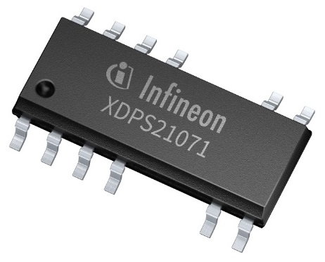
The XDPS21071 is a DCM flyback architecture digital PWM controller for high-density adaptor applications. A DSO-12 package includes a large feature set and only requires a few extra components. Advanced algorithms for multi-mode operation and protective features are provided by an integrated ASSP digital engine. Optimized high-density adapter system dimensioning is aided by forced frequency resonant operation. A one-time programmable (OTP) unit is also included, which provides a select set of adjustable parameters that may be tailored to a specific system design.
Specification
- Board Type: Fully Populated
- Current – Output:2.25A
- Frequency – Switching:140kHz
- Main Purpose: AC/DC, Primary and Secondary Side
- Outputs and Type:1, Isolated
- Power – Output:45W
- Regulator Topology: Flyback
- Supplied Contents:Board(s)
- Utilized IC / Part: XDPS21071
- Voltage – Input:90 ~ 265VAC
- Voltage – Output:20V
Features
- Multi-mode operation with BM, DCM
- Configurable ZVS-enabled line voltage
- ZVS gate drive signal for forced resonant mode
- Built-in soft-start
- Built-in protection modes
- Brown-in and brownout detection via integrated HV startup cell
- Pb-free lead plating; RoHS compliant
- Halogen-free according to IEC61249-2-21
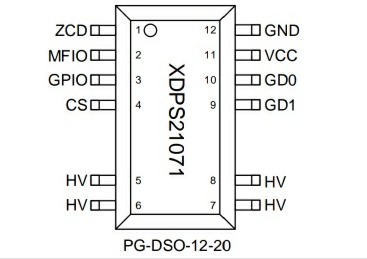
Pinout of XDPS21071
| Pins | Symbol | Type | Description |
|---|---|---|---|
| 1 | ZCD | Input | Zero-Crossing Detection. We connect the ZCD pin to an auxiliary winding for zero-crossing detection and positive pin voltage measurement. |
| 2 | MFIO | Input | Multi-Functional Input-Output. We connect the MFIO pin to an optocoupler that provides an amplified error signal for the PWM mode operation |
| 3 | GPIO | Input/output | Digital General Purpose Input Output GPIO pin provides a UART interface until brown-in. It is switched to weak pull-down mode and disabled UART function during normal operation. |
| 4 | CS | Input | Current Sense We connect the CS pin via a resistor in series to an external shunt resistor and the source of the power is MOSFET. |
| 5 | HV | Input | High Voltage Input We connect the HV pin to the rectified bulk voltage. An internally connected 600V. HV startup cell is used for the initial VCC charge. Furthermore, brown-in and brownout detection is provided |
| 6 | HV | Input | High Voltage Input |
| 7 | HV | Input | High Voltage Input |
| 8 | HV | Input | High Voltage Input |
| 9 | GD1 | Input | FFR Signal Gate Driver Output GD1 pin provides a gate driver pulse signal to start the forced frequency resonant mode operation |
| 10 | GD0 | Output | Gate Driver Output Output for directly driving the main power MOSFET. |
| 11 | VCC | Power Supply | Positive Voltage Supply IC power supply |
| 12 | GND | Supply | Power and signal ground |
Application and Uses
- Cell phones, mobile devices
- High-density chargers/adapters.