In this tutorial, we will make a “Half-Adder Circuit Diagram”. In the case of binary number addition, we only get two numbers either 1 or 0. An adder circuit is a combinational digital circuit that is used for adding two numbers. A typical adder circuit produces a sum bit denoted by “S” and a carry bit denoted by “C” as the output. In the binary number system, 1 is the largest digit. We only produce carry when the addition is equal to or greater than 1 + 1 and due to this, the carry bit will be passed over to the next column for addition. Adders can also be realized by adding other formats like BCD (binary coded decimal), XS-3, etc. In addition, adder circuits are used for a lot of other applications in digital electronics like address decoding, table index calculation, etc. The basic binary adder circuit is classified into two categories.
- Half Adder
- Full Adder
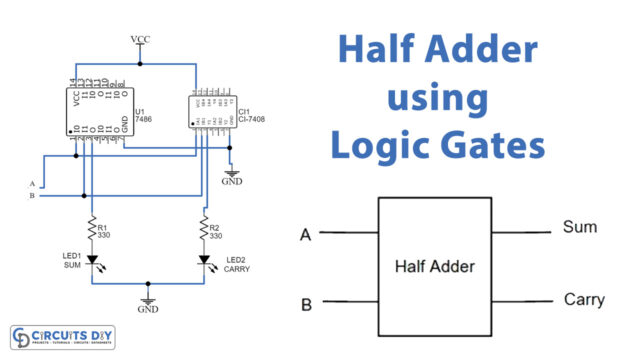
Here the two input and two output Half adder circuit diagram is explained with logic gates circuit and also logic IC circuits.
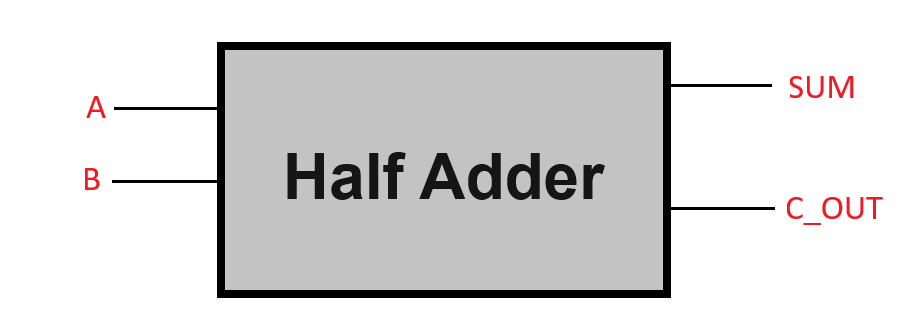
Half Adder
Half adder is a combinational circuit that is used to add two binary numbers of one bit each and generates the output as the sum and carries. It does not hold the ability to consider the carry-in generated from previous summations. In the present addend, when added with the augend. It provides sum and carries, which means not all summations bring a carry with them. However, if it holds a carry then the carry bit is represented as high otherwise low. Half adders are used in addition to the LSB of the numbers only.
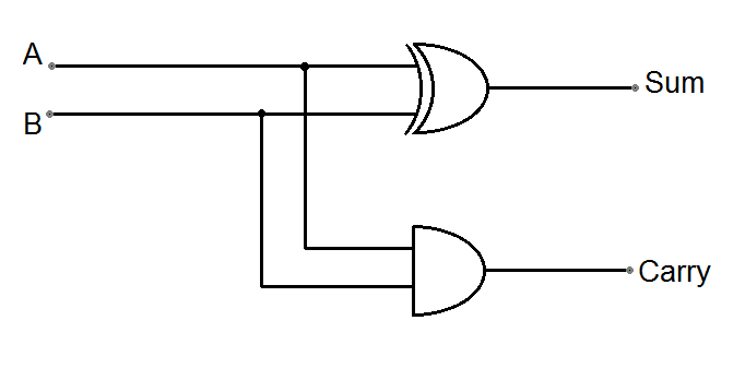
If half adder will take two inputs named A and, B then it will give two outputs named Sum, and Carry.
- Sum = A ⊕ B
- Carry = A . B
The result Sum is an exclusive addition between A and B, then the result in Carrying is AND logic operation between A and B.
Half Adder Logic Gate diagram
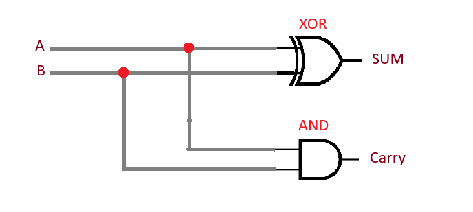
The Half Adder logic circuit could be constructed from two-input XOR gates and two-input AND gates. The applied inputs are the same for both gates present in the circuit. But the output is taken from each gate, where the output of the XOR gate is referred to as Sum, and the output of AND is known as carrying.
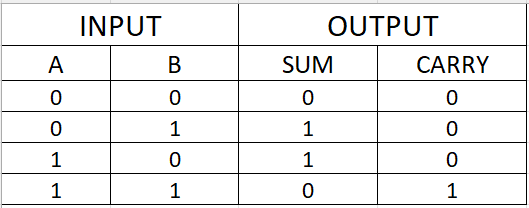
Half Adder Truth Table
The input & output of this logic diagram can be derived from the following truth table.
As we can see in the diagram, two gates are combined. The same inputs A and B are provided in both gates. Here we get the SUM output across the XOR gate, and the Carry out a bit across the AND gate.
The Boolean expression of the Half Adder circuit is-
SUM = A XOR B (A+B)
CARRY = A AND B (A.B)
When both inputs are low (A=0, B=0) then sum and carry will be logic low (0). If any one input is high (A=1, B=0 or A=0, B=1) then Sum will be logic high (1), and carry will be logic low (0). When both inputs are high (A=1, B=1) then Sum becomes logic low (0), and Carry becomes logic high (1).
Hardware Required
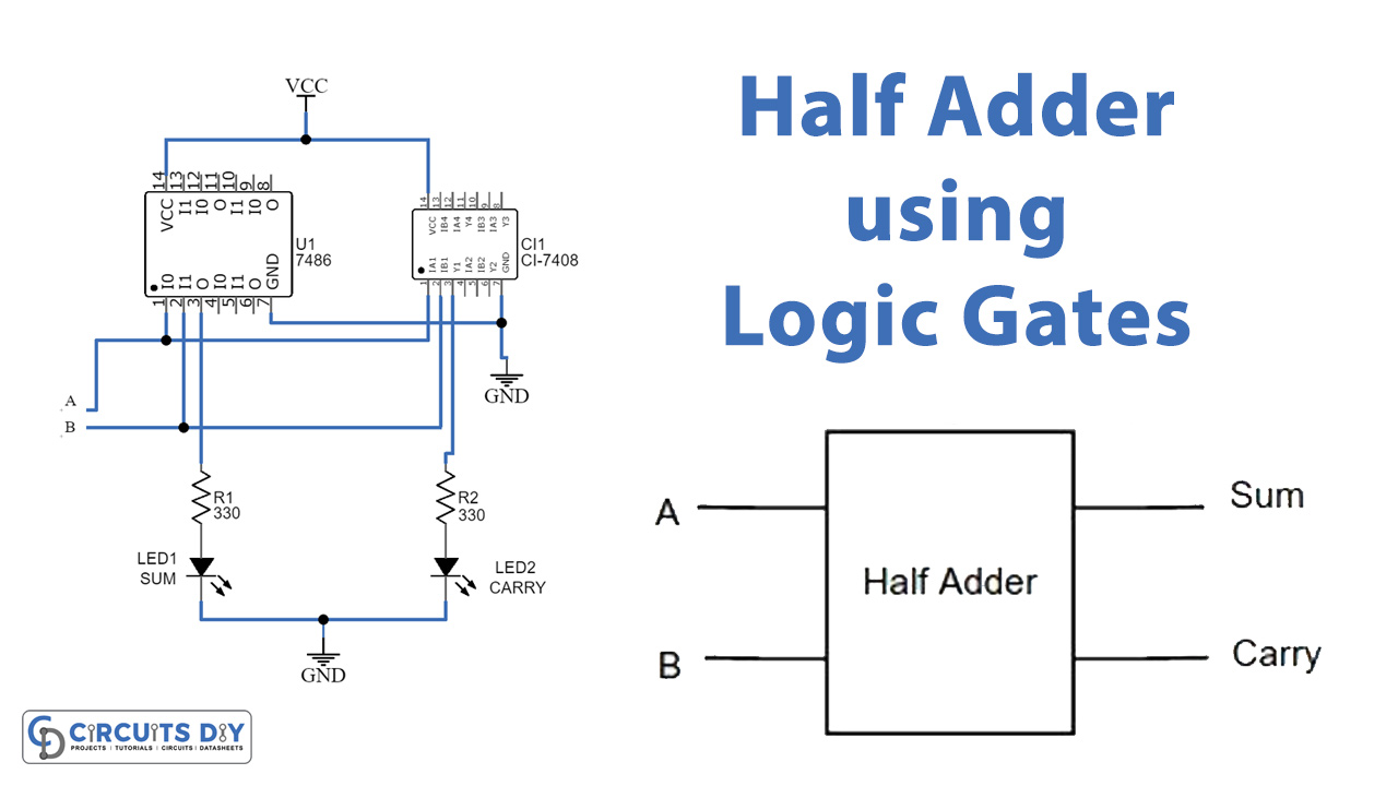
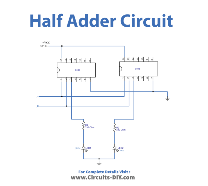
Circuit Diagram
Working Explanation
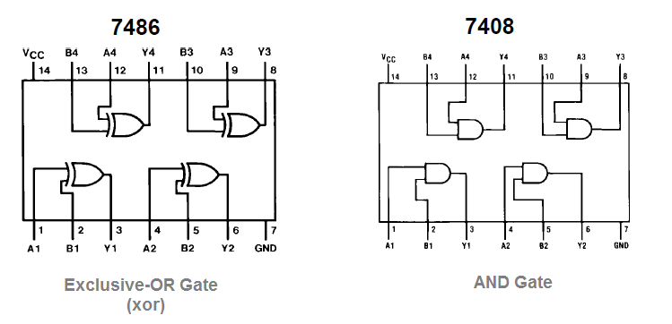
Here logic XOR gate IC 7486 and logic AND gate IC 7408 are used to make the half-adder circuit, both are quad 2 input logic gate IC. Pin 1 and 2 of 7486 are the input of the gate and pin 3 is the output of the gate. On the other side pin, 1 and 2 of 7408 are the input of the AND gate, and pin 3 is the output of the gate. Pin No 7 of both ICs is connected to GND and the 14th pin of both ICs is connected to VCC. First connect Vcc +5V and GND supply to logic IC, as both IC will give output at pin 3. Hence the XOR gate output is connected to the LED1 through the R1 resistor (Sum output indicator).
AND gate output is connected to the LED2 through an R2 resistor (Carry output indicator). Here when the LED glows it represents logic High (1), if the LED stays OFF then it represents logic LOW (0). Now connect Input A, B to +Vcc for logic High (1) input and connect Input A, B to GND for logic Low (0) input. Sometimes you can open A, and B terminal represents logic High.
Applications
It can be used in many applications like BCD (binary coded decimal), encoder, address decoder, binary calculation, etc.