Introduction
Since the world is increasing and technology is getting bigger, the devices are getting smaller. In past eras, the computers and other machines were bigger than today, but over time when technology gets improved and miniature components came in, the sizes become smaller, and now in this era, designers are trying to take things on the palm of our hands. Thus, SMT components and SMT PCBs play a good role in this. Companies like JLCPCB make it more convenient for engineers and designers. So, here in this article, we are going to discuss how PCB Manufacturing SMT Assembly has been Simplified by JLCPCB. But, before starting, let us discuss SMT technology.
Overview of SMT Technology
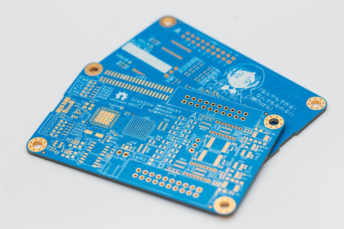
Surface Mount Technology is a method for constructing electronic circuits in which SMC components mount directly onto the surface of the Printed circuit board. Electronic devices made for this purpose are called surface mount devices or SMDs. In an SMT PCBA, the solder joint forms the physical & mechanical connections. Also, the bonding of the solder joint is to the surface of a conductive landing pattern.

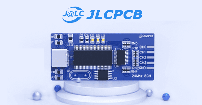
JLCPCB SMT Printed Circuit Boards
JLCPCB has expanded the number of SMT components available, improved the ordering procedure, and improved SMT quality while reducing turnaround time. J LCPCB was the first company to build a completely automated factory, to use an ERP system for online buying, and to have non-stop manufacturing.
How to get your SMT PCB Assembled?
Design Your PCB
To begin, go to the EasyEDA website and register for a free account. It is also possible to register and log in using a Google Account. We will now begin a new project and create our circuit schematic. Go to “Editor” and create a new project after you’ve logged in.
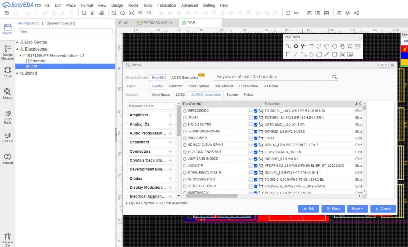
Selectig JLCPCB Assembly Parts
To create a standard SMT PCB, we must first pick the components needed for the project. It was simple in this case since JLCPCB provides a component library with all the necessary information.

The best thing is that these components’ footprints are available in EasyEDA, as seen below. Simply search for it and combine it with the component number you received from JLCPCB.
Components Placement and Routing
Locate the components in the library and drag them onto the canvas. Connect the components using the “Wire” tool. Save the circuit when you’ve done sketching it by clicking save.

Create PCB Layout
Now create the circuit’s layout.
from the top of the list of tools, select “Convert to PCB” from the convert button. This will result in a window. You may now insert the components inside the barrier and organize them as desired. Save once you’ve completed arranging all of the components. The “auto-route” technique is a simple approach to route all of the components. To do so, select “Auto Router” from the “Route” Tool.

Download Related Files
You may now get the Gerber file from JLCPCB and use it to create your PCB. The Gerber file provides information about your PCB, such as PCB layout, layer information, spacing information, and track information, to mention a few. Let’s put things in order now. The Bill Of Material (BOM) file includes a list of all the components in the Layout.
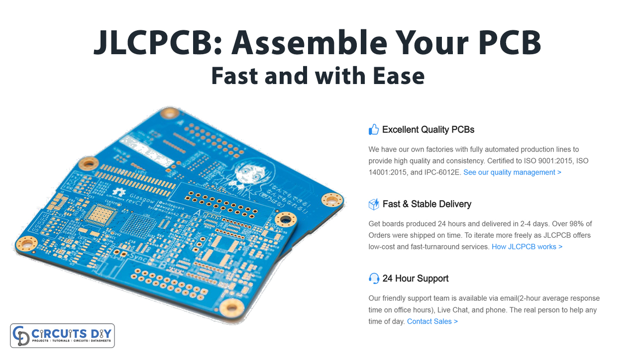
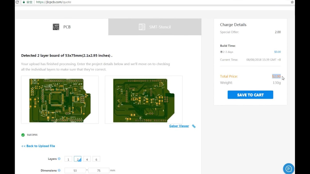
Go to JLCPCB and upload Gerber File
Go to JLCPCB, make an account, if you don’t have one. If you have already, log in to that account. After you’ve completed the registration process, click “Quote Now” and submit your Gerber File.

Assemble your PCB as SMT
Once you’ve uploaded the Gerber file, you’ll be able to get a preview of your circuit board. Make certain that this is the board’s PCB Layout.
There are numerous options below the PCB preview, such as PCB Quantity, Texture, Thickness, Color, and so forth. Choose everything that is required for you Now select “Assemble your PCB boards” from the drop-down menu.
Upload BOM and CPL Files
Now, upload BOM and CPL files that you have downloaded earlier.

Review and Save your Order
You may check the status of your order You may go over the layout and view all of the components, and if there are any issues, you can use the “Go Back” button to change your order. After that, save your order by clicking save to cart
Within days, the PCB will be built and dispatched, and it will be delivered to your door within the specified time frame.