Any industry that uses electronics must have a professional design for their circuit boards’ PCB layout to ensure they work well. Have you ever been curious about printed circuit boards (PCBs) and how PCB designers customize the layout? You might have many other questions about your thoughts at the moment. So, to learn about PCB design, let’s delve into this topic.
What Exactly is PCB?

Have you ever seen the green color board inside any electronic device or toy? That’s precisely what PCB is!
The abbreviation “PCB” stands for “printed circuit board,” It refers to a sheet of insulating material like fiberglass with a metallic circuit or track printed or etched on it to make it electrically conductive. You can find a printed circuit board in practically all the electronic items we use daily, such as our mobile phones, tablets, computers, laptops, keyboards, mice, aircraft, satellites, and military weapons.
Printed Circuit Board—What Is It Like today?

Almost everyone uses a gadget with a printed circuit board every day. There’s a good chance most people have them in nearly all of their electronic devices, even if they don’t realize it. PCBs are the brains of all modern electronics, from ordinary appliances to high-tech gadgets.
This demonstrates how PCB has evolved and continues to evolve through time, which is expected for all industries.
In the present PCB market, attention is mainly concentrated on pushing for smaller devices (miniaturization) which have resulted in astounding technical wonders and wearable smart devices.
Applications of PCB in Different Industries

PCBs have widespread applications across various industries, making them accessible in multiple products, from handheld electronics to industrial equipment. Here are some industries where Printed circuit boards are widely utilized in the modern world.
Consumer Electronics
Circuit boards (PCBs) are used in smartphones, laptops, and other everyday household items. PCBs are becoming more commonplace as more and more products use electronic components.
Despite their miniature size, today’s smartphones and laptops pack a surprising number of complex electronic components, necessitating PCBs with a high density of connections. Printed circuit boards (PCBs) used in consumer electronics must also be inexpensive to maintain competitive market pricing. Similarly, manufacturers value boards they can rely on since doing so is essential to keeping their businesses afloat.
PCBs are used in various consumer electronics products, such as:
- Smartphones, tablets, computers, laptops
- Smartwatches
- Radios and other communications products.
- Televisions,
- Video game consoles
- Refrigerators
- Microwaves
- Coffee or tea makers, etc., etc.
Modern Medicine
As time has progressed, the role of electronics in medicine has grown in importance. Technological advances in diagnosis and therapy have revolutionized patient care. Past developments have seen the introduction of several useful electronic products in the medical and healthcare fields, including:
- Responsive Neurostimulator
- MRIs
- CT Scans
- Ultrasound equipment
- Temperature monitors
- Blood pressure monitors
- Heart monitors
- Pacemakers
- Nerve Stimulator Unit
- Infusion fluid controls
- EMG activity systems
- X-ray computed tomography
- Peristaltic infusion technology
Industrial Equipment
PCBs are used in almost all industrial machinery and equipment. PCBs are growing increasingly complicated to fulfill more functions at quicker speeds and with more reliance as technology and the enormous electronics industry progress.
Hence, The industrial world has been taken over by printed circuit boards. PCB makers use different PCB assembly methods to make boards that are strong enough for a wide range of demanding industrial applications. Some of the industrial application examples are:
- Conveyer belts
- Cranes
- Electric drills and cutters
- Electric scales
- Flow sensors
- Liquid level meters
- Temperature monitoring and logging systems
- Servo Motor Driver
- IInverters
- Three-phase Power controller
- PLCs and SCADA.
Automotive Industry
Vehicle-printed circuit boards are developed to accommodate various applications and real-world conditions. This board connects the electrical components of the car’s radio and video display gadgets to ensure proper operation. The GPS makes use of printed circuit boards designed for automobiles. In addition to these uses, some more applications are:
- Antilock brake systems
- Engine coolant level monitors
- Engine timing systems
- LED brake lights
- Power distribution junction box
- Remote diagnostic systems
- Security systems
- Transmission sensors
- Ignition systems
- Transmission sensors
- Windshield wipers
Security and Saftey Devices
Manufacturers across many sectors need PCBs for products that prioritize safety and security. Providing public safety and service, employee safety, and assisting businesses in meeting and exceeding corporate responsibility requirements and objectives are just a few of the many critical roles that these applications play in maintaining the safety and security of everyone involved.
Products and systems for safety and security, which often involve PCBs, including
- CCTV systems
- Public address systems
- Door alarms
- Fire safety management
- Road safety system
- Intruder and burglar alarm devices
- Proximity sensors
Aerospace Industry
Manufacturers across many sectors need PCBs for products that prioritize safety and security. Providing public safety and service, employee safety, and assisting businesses in meeting and exceeding corporate responsibility requirements and objectives are just a few of the many critical roles that these applications play in maintaining the safety and security of everyone involved.
Some of the aerospace applications are:
- Radio communication systems
- LED lighting systems
- Signal sensors
- In-flight power supplies
- Control tower systems
- Radar installations
- Power converters
Maritime Applications
PCBs are vital to the operation of many maritime ships and equipment types. In the same way, as aircraft PCBs must survive extreme temperatures and pressures, so must marine PCBs. Because it is crucial for the safety of the crew and passengers that electronic equipment functions correctly, manufacturers of marine printed circuit boards place a strong emphasis on reliability.
Here are some of the maritime applications:
- Communication systems
- Navigation systems
- Control systems
- Power distribution system
- Autopilot system
Print circuit boards are used in various maritime applications, making it crucial to find a PCB manufacturer willing to deal with specific requirements.
PCB Design Services: How Do They Work?

There are a lot of steps involved in PCB design. If the design is brilliant, one may create a printed circuit board that will work well and last a long time. For the sake of clarity, we’ll outline the primary stages of the design process here:
Building a Schematic
The schematic represents the simple layout of your circuit. The placement of the components and the connections between those components are both parts of the building of the schematic. Regarding the components, almost every software comes with hundreds or thousands of libraries. In addition, you may create your own design and implement it as a component of your project. This will provide your designs with more flexibility.
PCB Stackup
The rapid advancement and sophistication of consumer electronics demand precise multilayer PCBs. To avoid complications, stacking has recently gained popularity. The current PCB design method begins with FR4 material, a two-layer to sixteen-layer board utilizing a stack-up library that may assist you in grasping various laminates and unique materials if you need to familiarize yourself with the technique.
Creating a Layout
Although creating a schematic may not be challenging, it is much simpler to transform it into a board layout. The ideal PCB layout designer will be able to demonstrate how precisely your board will function.
After the schematics are made, reviewed, and approved, and the layer stack is set, component models are imported into a PCB layout for placement and routing. First, the board size is determined by the mechanical requirements. The essential components are included in the PCB layout to assure external and internal connection and solvability during routing. Choosing where to put components may ease routing and assist in avoiding issues like EMI, SI, PI, etc.
Routing
The traces, rails, transmission lines, and other printed circuit parts are routed around the board to finish the necessary connections in the PCB layout. If you want your device to meet standards for signal integrity and power integrity, you need to pay close attention throughout the routing phase.
Device-Specific Regulations
Although many PCB rules are available, not all of them need to be included in the final design. They can adapt the set of rules to the specific device being manufactured. This step is mainly about the IPC standards for Component Footprint and PCB Fabrications, which are the standard rules for making PCBs and other electronic devices.
If the stages that came before it are finished correctly, the phase of PCB routing will be considerably simpler, and there will be less need for rework.
Simulation Verification
After the PCB layout is complete, verification is necessary for complex items. To do this, electromagnetic simulation software is used. You may use these tools to detect signal integrity, power integrity, and EMI issues, which might cause EMC or performance failure during operation.
Design Review
After completing the PCB design, you must conduct a final design review to guarantee that all mechanical, electrical, and performance specifications have been satisfied. Design evaluations are highly recommended at every level of the PCB design process.
Reviewing the PCB design often helps catch any flaws early and ensures that the device meets all of its functional criteria. During this stage, issues such as the design for testing may be examined, which is particularly useful if a prototype version of the board is being built.
File Creation for Manufacturing
PCB manufacturing files must be generated when the design has been finalized and accepted. The majority of PCB manufacturers will not utilize your native ECAD files throughout the fabrication and assembly of your PCB. Files are used inside to make tools and code the automated processing equipment. Therefore, the primary set of outputs required by PCB manufacturing and assembly facilities to manufacture a PCBA is:
- The Gerber file has all the information about the board’s layers, widths, dimensions, and traces.
- Files CPL and BOM
- NC drill data.
- PCB fabrication and assembly drawings with notes detailing specifications.
- A BOM containing component source details.
After preparing these files, you can deliver the design to the manufacturer for a price estimate and DFM analysis. As part of a DFM analysis report, a manufacturer may request modifications to meet product acceptance and inspection criteria.
Types of PCBs to Design

Different types of PCBs exist because of differences in industry standards, manufacturing methods, and product requirements. Various PCB service boards become possible as PCB designs get more complicated. Additionally, the PCB design services price will change based on the layer selection.
Space, stress tolerance, and mechanical and electrical reliability are just a few factors to consider when deciding on a printed circuit board (PCB).
Single Sided PCB
A single-layer PCB is a printed circuit board (PCB) with only one layer of conducting material on one side of the board. The other side of the board incorporates various electronic components onto the board. A single-sided PCB is another name for a single-layer PCB.
Even though they were the foundation upon which printed circuit board technology was built, single-layer PCBs are still an essential component of the electronic sector.
Advantages
- Low Cost: The price is much lower than other types of PCBs. Because it has just a single layer
- Simple Design: The design is simple because there is just one layer. As a result, a PCB of this kind is simple to assemble. In addition, the likelihood of my accuracy in this scenario is quite remote.
- Easy to troubleshoot: Circuits created on this PCB are both tiny and straightforward, making it easier to troubleshoot any problems that may arise.
Applications
- Photocopy and printer machines
- Vending machine circuits
- Solid-state devices and equipment
- Digital and analog power supply
- Digital cameras circuits.
- Radio and stereo equipment’s circuits.
- Photocopy and printer machine circuits.
- LED lighting circuits.
- Timing circuits.
- Surveillance machine circuits.
Double Layer PCB
A printed circuit board known as a double-sided PCB has a copper coating on all four sides, including the top and bottom. Since it is possible to plan and solder on both sides, it is frequently utilized since the complexity of the layout is substantially reduced.
Advantages
- Flexible: More flexibility for designers.
- Affordable Cost: Costs that are, on average, not as high
- Simple: The complexity level of the circuit is intermediate.
- Reduced Size: Scaling down the size of the boards
Applications
- Monitoring system
- Amplifiers
- Industrial controls
- Power supplies
- UPS systems
- Hard drives
- Automotive dashboards
- Line reactors
- Test equipment
- Amplifiers
Multilayer PCB
In contrast to a double-sided printed circuit board (PCB), which only consists of two layers of conductive material, a multilayer PCB must include at least three layers of conductive material, all of which are positioned in the material’s center.
Advantages
- Light Weight: Multi-layer PCBs are more lightweight than other PCBs. Circuits decrease or remove connectors. Reduce building complexity. This increases circuit mobility. So, better for electronics.
- Small Size: The design makes these PCBs compact. Modern electronics need smaller sizes. Electronics are shrinking. Compact PCBs help make smaller gadgets.
- High durability: Multilayer PCBs resist pressure and thermal expansion. It improves circuit durability.
- Powerful: Multiple layers are printed on one board. Because of their high assembly density, they can hold more.
- High Speed: Close quarters help the board to be more connective—increase speed.
Applications
- Computers, laptops,
- GPS technology
- Handheld devices
- Test equipment
- X-ray equipment
- Heart monitors
- Atomic accelerators
- Nuclear detection systems
- Space probe equipment
Rigid PCB
Rigid printed circuit boards (PCBs) are a kind of circuit board that cannot be flexed or bent due to their rigid, inflexible construction. Substrate, copper, solder mask, and silkscreen are only some of the layers that go into their construction, and they’re all adhered and bonded using heat and adhesive.
Advantages
- Small Size: The rigid PCB’s small size is a benefit. The PCB’s small size allows complicated circuitry to be built around it. It reduces equipment space.
- Noise Reduction: The PCB is intended to decrease electronic noise. Electrical currents between the circuit board’s electronic components are reduced. This reduces radiation. Low electric and radiation currents entail less electromagnetic.
- Low Electronic Noise: The PCB is made to have as little electronic noise as possible in an application. Rigid PCB helps to achieve this.
- Easy to troubleshoot: The way these PCBs are made makes them easy to fix and maintain
Applications
- Computer motherboards.
- Desktop devices.
- Solid state devices.
Flex PCB
Flex-printed circuit boards, also known as flexible printed circuits (FPCs), are situations where a rigid circuit board would be impractical. Since it is made of flexible materials, a flex PCB is more resilient to mechanical stress and vibrations than other designs.
Advantages
- Reduce Size: Combining flex circuits with rigid boards simplifies design and reduces package weight and size. You may develop device-specific circuits.
- High-density components: Certain applications demand rigid-flexible PCBs with high component density since rigid and flexible circuits alone can’t meet project requirements.
- Fewer connections: Rigid-flexible PCBs need fewer connections, components, and connector assembly. Productivity rises.
- Reduce Vibration and Shock: Resonance reduces vibration and stress on heavy electronic components. Rigid-flex PCBs can withstand high temperatures, radiation, heat, shock, and other harsh circumstances.
Applications
- Calculators
- Wearable electronic
- Smartphones
- Printers
- LCDs
- Cameras
- Pacemakers
- Hearing aids
- Robotic arms,
- Processing machines
- Bar code equipment
Rigid Flex PCB
These hybrid rigid-flex printed circuit boards combine the advantages of both flexible and stiff boards. Depending on the intended use, rigid-flex boards may have one or more rigid boards mounted to the outside of many layers of flexible circuit substrates.
Advantages
- Size Reduction: Compact rigid-flex PCBs are utilized for product miniaturization. It fits readily in tiny electrical devices. Thus it’s used to create complex circuits.
- Save Money: Since rigid PCBs are easier to manufacture, their prices tend to be higher than those of rigid-flex PCBs. However, rigid-flex PCBs have the potential to cut down on production costs.
- Easy Testing: Because all the subcircuits are linked during the production of the PCB, automated testing of a rigid-flex PCB is simple.
- Improve reliability: Connectors are helpful when frequently disconnecting the wire harness from the PCB is necessary, helping to improve reliability.
Applications
- Mobile phones
- Digital cameras
- Pacemakers
- Cochlear implants
- Handheld monitors
- Communication systems
- GPS
- Aircraft missile-launch detectors
- surveillance or tracking systems,
- Electronic control module
- Transmission controls
- LCDs
- Air conditioning systems
- TV remote controller
Guidelines for Creating an Exceptional Printed Circuit Board
We have included some helpful tips below, for those who are just starting in printed circuit board design.
Placement of Components
The correct positioning of the components on the PCB is essential, as it avoids the arising of problems that could compromise the manufacturability, functionality, duration, and maintenance of the printed circuit board
To achieve optimal performance, the precise positioning of each component is an art form that needs careful adjustment. Arranging each component is challenging; therefore, keeping the standards in mind when developing the PCB layout is essential.
Space between each Component
It’s essential to know how much space is required between each component. The greater the number of components on the board, the greater the range of functions a single device may perform. As the number of components on a circuit board increases, it becomes more difficult for the designer to maintain enough clearances for wire routing and to prevent the board from overheating.
Traces
Now that everything is where it needs to be, including enough room between components, the power and signal lines can be routed. If your board forces for a horizontal trace, you must route the traces vertically on the other side, as shown in the figure below.
Avoid potential heating problems
The constant struggle against heat is a continuous challenge with PCB. YOu may solve the heating problems in various ways, including providing enough separation between components rather than stacking them near one another.
Locations of Test Points
Many problems with the design may be worked out using this kind of testing. Accurate and convenient test points placement is essential. It will be challenging to test if you reach the places to be tested. You can resolve all testing problems if access to test locations is optimized.
Wrapping up: PCB Design
It is possible to achieve a successful printed circuit board by adhering to the procedure and efficiently designing the stack-up.
With these considerations out of the way, manufacturing and production begins. After the printed circuit board (PCB) is assembled, product engineering services may assist with testing the finished product to guarantee that the new product is ready.
Related posts:
 Top 5 PCB Design Issues Faced In PCB Manufacturing & Their Solutions
 JLCPCB: 2$ Purple Solder Mask Printed Circuit Board - PCB
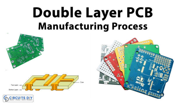 Double-layer PCB- Manufacturing Process
 Laser Tripwire Security Alarm Using NE555 Timer IC
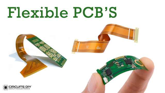 How To Make Flex PCBs At Home - A Beginners Guide
 PCB Design Issues Faced In PCB Manufacturing & Their Troubleshooting


