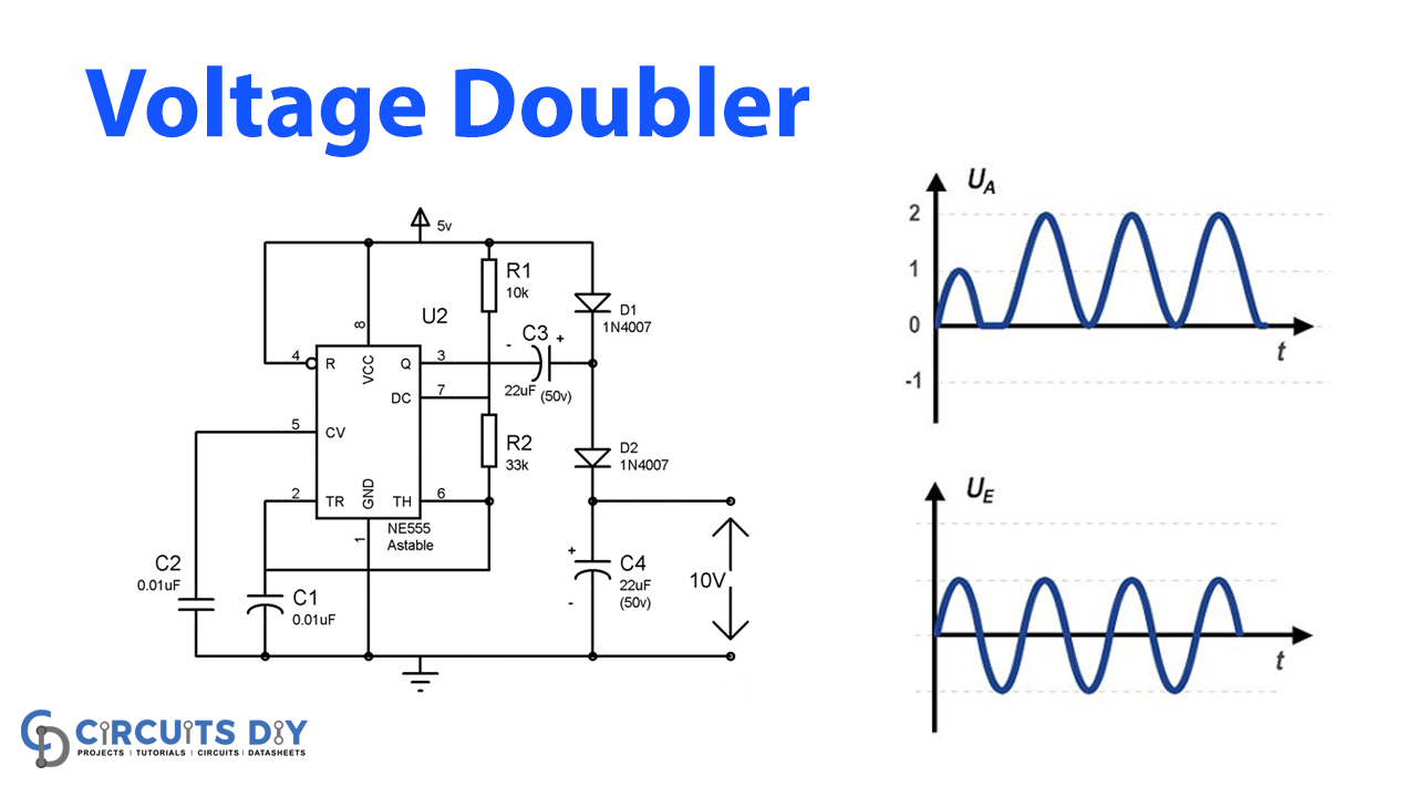
In this DIY circuit tutorial, we have come up with an astounding circuit that is widely used in electronic devices, it is the Voltage Doubler Circuit. However, the Voltage doubler circuit utilizes to get twice the input voltage. For example, if we supply an input voltage of 5 volts, it will subsequently provide 10 volts at the output.
Therefore, this circuit is frequently used as a transformer whose primary function is to either step up or step down the voltage. Yet some of the time transformers are not possible to afford because of their size and cost. So here is the snappy, simple, and handy solution for getting a voltage doubler circuit. Meanwhile, the circuit is built by using a NE555 timer IC and a few other components.
Hardware Components
The following components are required to make Voltage Doubler Circuit
| S.no | Component | Value | Qty |
|---|---|---|---|
| 1. | Diode | 1N4007 | 2 |
| 2. | Resistor | 10K, 33K | 1, 1 |
| 3. | Electrolyte Capacitor | 22uF | 2 |
| 4. | Ceramic Capacitor | 0.01uF | 2 |
| 5. | Power supply source | 3-12 V | 1 |
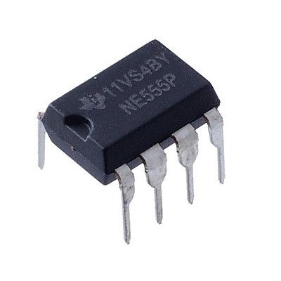
| 6. | IC | NE555 timer | 1 |
NE555 IC Pinout
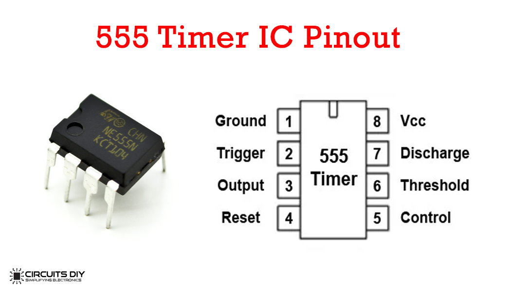
For a detailed description of pinout, dimension features, and specifications download the datasheet of 555 Timer
Voltage Doubler Circuit

Working Explanation
To better comprehend the circuit operation, we can partition the circuit into two sections. The first section comprises the 555 timer IC in Astable mode, to create the square wave, however, the second part shall consist of 2 diodes and 2 capacitors to twice the yield voltage. We have arranged a 555 Timer IC in Astable multivibrator mode to produce square waves of approximately 2KHz. However, this frequency might be chosen by the resistors R1, R2, and capacitor C1. The following are the formulae for the equivalent:
F = 1.44/(R1+2*R2) * C1
At the point when the yield at PIN 3 of 555 IC is low, Diode D1 gets forward bias and capacitor C3 gets charged through the D1. Capacitor C3 gets energized to a similar voltage at the source, for our situation 5v.
Additionally, when yield at PIN 3 goes high, D1 gets reverse bias and hinders the discharging of the capacitor C3, and simultaneously D2 is forward biased and permits the capacitor C4 to charge. Although, the capacitor C4 accuses of the combined voltage of Capacitor C3 and the input source voltage, which implies 5v of capacitor C3 and 5v of input power supply. Thus, it energizes to 10v (double the voltage). However, in commonsense, we get a yield voltage not precisely twice the input voltage, as for our situation we get approx. 8.76v rather than 10v.
Applications and Uses
- It uses as an alternative to heavy and bulky transformers.