74LS256 belongs to the 74XXYY IC series. 74LS256 is a Dual 4-Bit Addressable Latch with common control inputs; these include two Address inputs (A0, A1), an active LOW Enable input (E), and an active LOW Clear input (CL). Each latch has a Data input (D) and four outputs (Q0–Q3). The 74LS256 IC has a wide range of working voltage, a wide range of working conditions, and directly interfaces with CMOS, NMOS, and TTL. The output of the IC always comes in TTL which makes it easy to work with other TTL devices and microcontrollers. The IC offers a wide array of features such as variable operating voltages & thermal overload protection.
What is a Latch Circuit?
A latch is a device that can be used to store one bit of information. The D latch is used to capture, or ‘latch’ the logic level which is present on the Data line when the clock input is high. If the data on the D line changes state while the clock pulse is high, then the output, Q, follows the input, D. When the CLK input falls to logic 0, the last state of the D input is trapped and held in the latch.
74LS256 Key Features & Specifications
- Technology Family: LS
- VCC (Min): 4.75V
- VCC (Max): 5.25V
- Bits (#): 4
- Voltage (Nom): 5V
- Serial-to-Parallel Capability
- Output From Each Storage Bit Available
- Random (Addressable) Data Entry
- Easily Expandable
- Active Low Common Clear
- Input Clamp Diodes Limit High Speed Termination Effects
- Frequency at operating voltage (Max): 35MHz
- Propagation delay (Max): 40ns
- IOL (Max): 16mA
- IOH (Max): -0.8mA
- Operating temperature range (C): 0 to 70
74LS256 Pinout
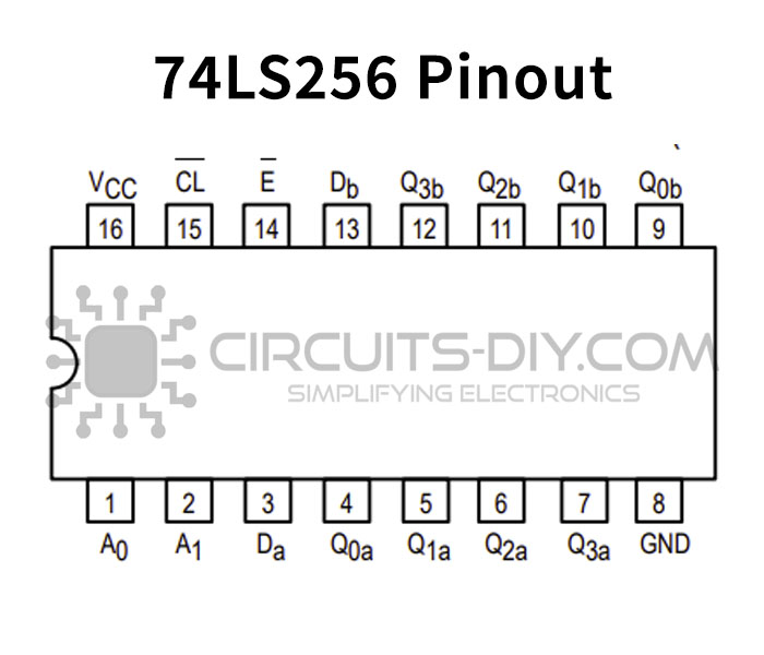
| Pin No. | Pin Name | Description |
|---|---|---|
| 1 | A0 | Address Input pin A0 |
| 2 | A1 | Address Input pin A1 |
| 3 | Da | Data Input pin A |
| 4 | Q0a | Parallel Latch Output Q0a |
| 5 | Q1a | Parallel Latch Output Q1a |
| 6 | Q2a | Parallel Latch Output Q2a |
| 7 | Q3a | Parallel Latch Output Q3a |
| 8 | GND | Ground Pin |
| 9 | Q0b | Parallel Latch Output Q0b |
| 10 | Q1b | Parallel Latch Output Q1b |
| 11 | Q2b | Parallel Latch Output Q2b |
| 12 | Q3b | Parallel Latch Output Q3b |
| 13 | Db | Data Input pin B |
| 14 | E’ | Active low Enable pin |
| 15 | CL’ | Active Low Clear pin |
| 16 | Vcc | Chip Supply Voltage |
Applications
The 74LS256 has a great number of applications. A few of them are mentioned below:
- Latch circuits are widely used in computing as well as data storage applications
- They are also used in circuits such as power gating & clock as a storage device.
74LS256 Datasheet
You can download the datasheet for 74LS256 Dual 4-Bit Addressable Latch IC from the link given below:
See Also: 74LS135 Quad 2-Input XOR Logic Gate IC – Datasheet | 74LS150 16-1 Data Selector Multiplexer IC – Datasheet | 74LS73 Dual JK Negative Edge Triggered Flip-Flop IC – Datasheet