The process of PCB soldering has a great impact on the quality of the finished PCB. Poor soldering practices and bad solder joints can severely affect the standard of your PCBs & can also make you lose your client’s trust. Even though the process of soldering is pretty straight forward, it requires constant practice in order to gain mastery in it. When we look at the different types of PCB soldering practices and techniques. It becomes quite understandable why the process might seem a bit daunting at first to beginners, and mistakes are bound to happen. In this guide, we will go over some of the common soldering issues that you may face and how you can resolve them.
JLCPCB is the foremost PCB prototype & manufacturing company in china, providing us with the best service we have ever experienced regarding (Quality, Price Service & Time).
Ideal Solder Joints vs Bad Solder Joints
Ideal Solder Joint
The Ideal Solder Through Hole Joint is similar to the shape of a Hershey’s Kiss
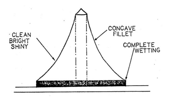
The ideal solder joint for THT PCB parts is basically a concave shaped fillet. It has a smooth & shiny exterior, pointed out at an angle of 40° to 70° from the base of the PCB. It basically looks just like a Hershey’s kiss. This shape is easily achievable by simply keeping the soldering iron at the right temperature, and also with proper cleaning of the oxidation layer from the PCB contacts.
So, the basic attributes of an ideal solder joint are:
- complete, solid solder wetting.
- Has a neat Concave fillet
- is properly clean and shiny
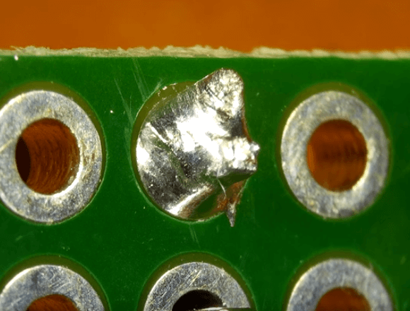
Bad Solder Joint
Regrettably, there are many ways for solder joints to go horribly bad. Soldering defects can occur due to a wide variety of reasons, ranging from worker errors to impurities present in the environment. Following are some common PCB soldering defects and methods to resolve them.
1) Cold Solder Joints
The reason behind the occurrence of cold solder joints is the lower than the optimal temperature of the soldering iron or the time period for joint heating was too short. The surface of the cold solder joint usually appears as dull, lumpy, and with pock marks.
Solution: To fix cold solder joints, simply reheat the joint with a hot soldering iron until the solder flows. In order to prevent this from happening in the future, make sure that the soldering iron is at soldering temp before use.
2) Overheated Solder Joint
By cranking up the heat way too much on your soldering iron, you subject your PCB board to burnt joints. Burnt solder joints appear as white soler joints, with no metallic luster and a rough outer surface. Burnt solder creates a tendency for solder pads to lift entirely from the surface of the PCB board. This will most likely kill your board and will require costly repairs.
Solution: In order to fix burnt solder joints, carefully scrap the tip of the overheated joint with the tip of a knife or small amount if isopropyl alcohol & a toothbrush to remove the burnt flux.
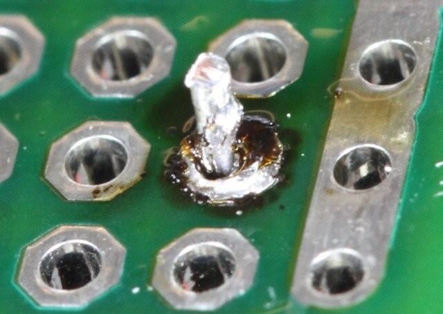
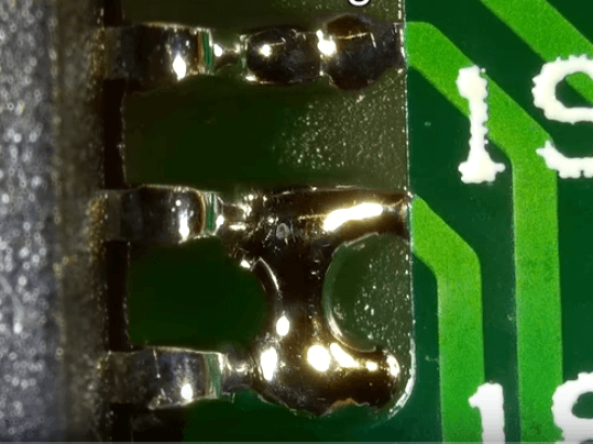
3) Solder Bridges
A solder bridge occurs when two or more points on a PCB board, that should not be electrically connected with each other, become accidentally short during PCB soldering. Solder bridges can occur due to two reasons: either due to excessive solder between joints or by using soldering tips that are far too wide. They are quite dangerous for the health of your board and if left undetected can cause the board to short circuit and burn out.
Solution: Gently draw away the excess solder by dragging the tip of the hot soldering iron between the two joints. Similarly, you can also use a sucker or a solder wick to get rid of the excess solder.
4) Webbing & Spatters
Webbing and solder spatter occur when you are using an insufficient amount of flux while soldering or when there is a presence of pollutants on the surface of the PCB board. Webbing and solder splashes are a major short circuit hazard that can damage the board.
Solution: Simply use use a sharp knife or a pair of tweezers to get rid of webbing.
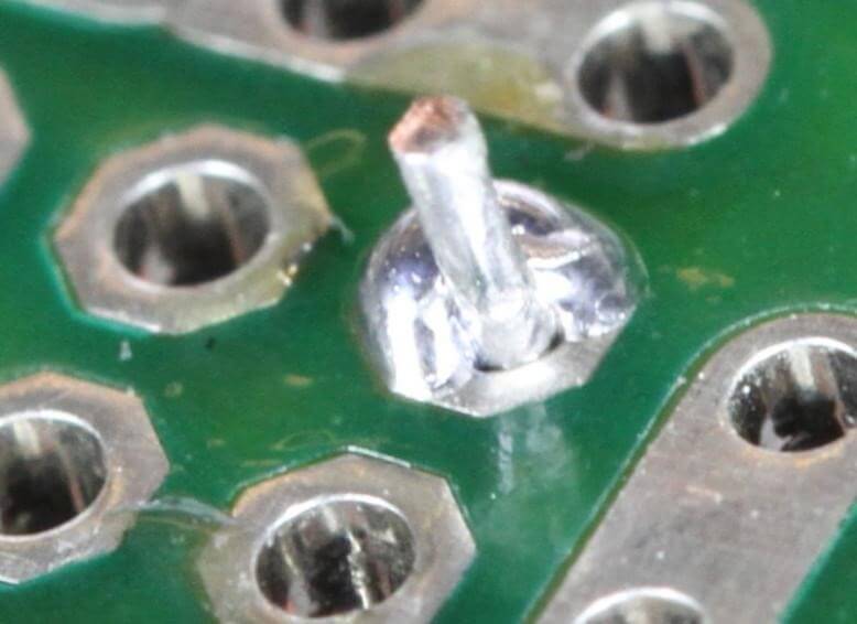
5) Insufficient Wetting (THT)
Insufficient wetting means that a solder joint has less than necessary solder to make a secure connection between the soldering pad & component attached to the PCB by the solder. Ideally, the solder should achieve 100% wetting with the solder pad & pin, with no gaps or spaces exposed. Insufficient wetting occurs due to the failure of applying a sufficient amount of heat to the pad and the pin. This limits & impairs the performance of the PCB.
Solution: To fix this, simply reheat the solder joint and apply more solder. Make sure that the tip of the iron is in contact with both the pin and the pad.
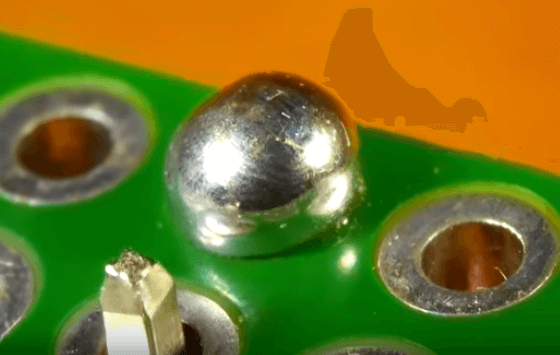
6) Too Much Solder
If during the soldering process, you notice a large bubble forming on the solder joint then you have probably used too much solder. The direct reason for this problem is simply the late withdrawal of the solder. it may be possible that the joint is securely connected with the pad, but it becomes very difficult to determine this beneath the mass of the solder.
Solution: Draw of the excess solder with the tip of the hot iron. Similarly, you can also use a solder sucker or a solder wick.
7) Lifted Pads
Lifting of solder pads occurs when the solder joint goes through extreme physical or thermal stress during soldering. A lifted pad is basically a solder pad that gets detached from the surface of the PCB. Lifted solder pads are exceptionally difficult to work with since the pad is very fragile and can easily tear from the surface of the trace.
Solution: It’s usually not very visually appealing to repair a lifted pad. The simplest repair you can perform is to fold the lead over to a still-attached copper trace and re-solder it.