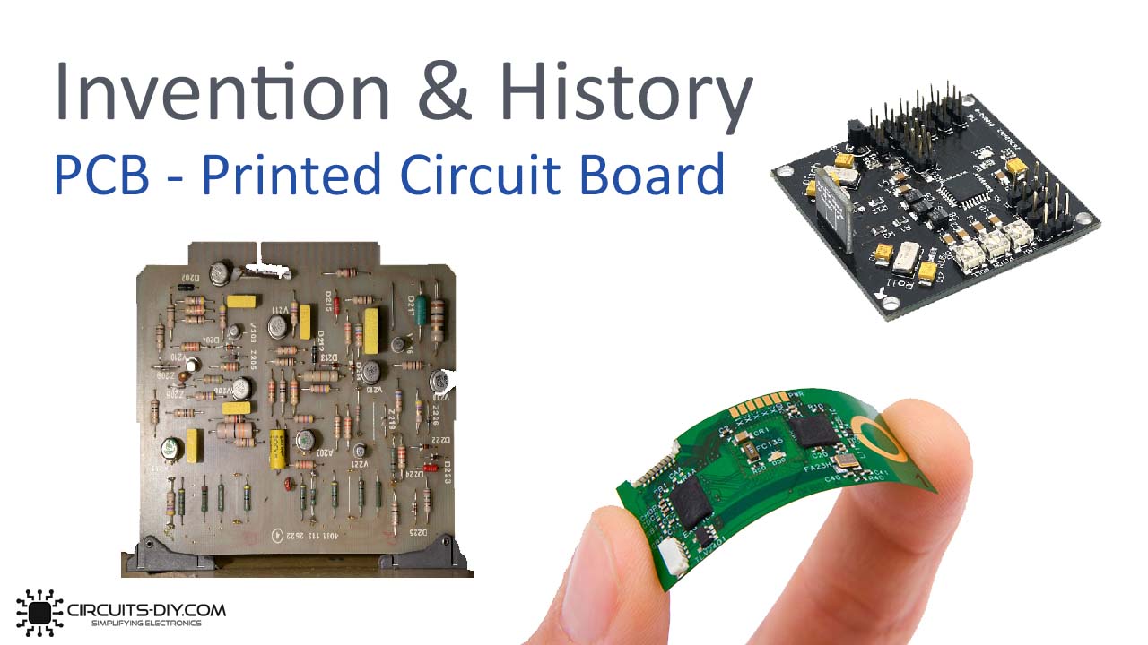
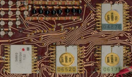
Introduction to Printed Circuit Boards
To make an electronic device, the printed circuit board plays a central role. It follows the design process that converts an electronic schematic (designed by the circuit designer) into a physical circuit board. However, there are three different ways to design the PCB, a single-sided PCB, a double-sided PCB, and a multi-layer PCB. These three types used two kinds of technologies, the through-hole technology, and the surface mount technology. But, these technologies got formulated by the long process of inventions in history. So, in this article, we’ll discuss the invention and history of the PCB.
The invention of the PCB
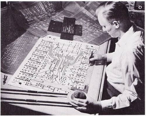
Before the invention of the PCB construction, the point-to-point formation was common for the printed circuit board. However, it was not significant and very questionable. To make the circuits more valuable, designers took the suggestion of making PCB board
Therefore, In the 1920s designers uses baseline or old thin pieces of wood. And, the holes were drilled into that wood material. And flat brass wires utilized onto it. The first application of those boards were gramophones and radios.
Then the invention of Printed Circuit Boards happened. The first PCB was developed in 1936 by Austrian designer Paul Eisler. At that time, it was designed to operate radio systems. Meanwhile, the United States military adopted this method. And, utilize this in proximity fuses in world war two. In 1948 this printed wiring board started to evolve.
History of the PCB
The designer, Eisler in the 1940s invented the more creative design of PCB. It includes the etching of circuits onto the copper foil. In the 1950s when the transistor got introduced in the market, the design got more modification. Since the translator have small in size so PCB got improved. After that, PCBs get advanced into a double layer. That contains electronic components on one layer and printing on the other side. Therefore, to prevent boards from degradation, zinc plates, and resistant material got introduced. Then, In the 1960s printed circuit boards are wrongly associated with the harmful chemical polychlorinated biphenyl.
To clarify, PCB is renamed as PWB, that is Printed Wiring board. Afterward, a new standard method for designing was discovered. Now, photo imageable polymer coating is applied directly to circuits. In the 1980s, surface mount technology was discovered. Before that technology components were soldered into the holes. On the other hand, in SMT components were soldered directly into small pads. Without the need for holes. It gets more popular as this technology was more reliable and has a low cost. In the 1990s the size of the Printed circuit board gets reduced. As a result, it improves reliability. In the 2000s it becomes smaller. Flexible and multilayer become more prominent. Most electronic devices used this for high speed.
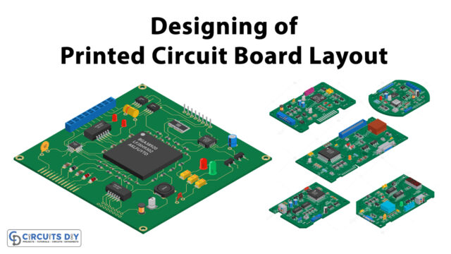
The PCB of the modern era is largely employed in the electronic industry. Single-layer, double layer, multi-layer, rigid, flexible. Every kind of different PCBs is used for different purposes. PCBs are now evolving and growing day by day.

Conclusion
We have discussed the invention and history of PCB. In conclusion, we can say that the invention of the PCB made the designer’s lives easier. Since Printed circuit boards have evolved a lot. But, still growing. Because technology can’t stop the process of evolvement. There is always some space for growth.