In this tutorial, we are going to make a “Boost Converter Circuit 555”.
We’ve all come across pesky situations where we need a slightly higher voltage than our power supplies can provide. We need 12 volts but have only a 9-volt battery. Or maybe we have a 3.3V supply when our chip needs 5V. That too, in most cases, the current draw is quite decent, we can achieve it by boosting the converter. A boost converter is a DC-to-DC power converter that steps up voltage while stepping down current from its input supply to its output load. It is a class of switched-mode power supply containing at least two semiconductors a diode and a transistor and at least one energy storage element: a capacitor, inductor, or the two in combination. To reduce voltage ripple, filters made of capacitors sometimes in combination with inductors are normally added to such a converter’s output load-side filter and input supply-side filter.
Boost converters are highly nonlinear systems and a wide variety of linear and nonlinear control techniques for achieving good voltage regulation with large load variations have been explored. They’re called switch-mode because there’s usually a semiconductor switch that turns on and off very rapidly. We design a boost converter circuit based on timer IC 555 and a few easy-to-available external components. In this boost converter circuit, IC 555 is configured in Astable multivibrator mode and we can adjust the output voltage by varying the output pulse frequency of the timer IC.
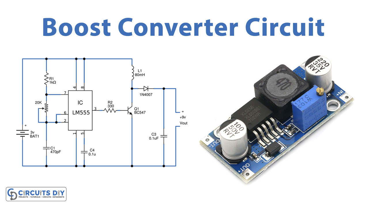
This circuit is designed to provide 9 Volt output from a 3-volt input power supply. If you need high voltage from a 3-volt battery you can use this circuit to boost supply voltage.
Hardware Components
The following components are required to make Boost Converter Circuit
| S.no | Component | Value | Qty |
|---|---|---|---|
| 1. | IC | NE555 timer | 1 |
| 2. | Transistor | BC547 | 1 |
| 3. | Diode | 1N4007 | 1 |
| 4. | Variable Resistor | 20KΩ | 1 |
| 5. | Resistor | 1KΩ, 330Ω | 1,1 |
| 6. | Ceramic Capacitor | 470pF, 0.1µF | 1, 2 |
| 7. | Inductor | 80mH | 1 |
| 8. | Connecting Wires | – | 1 |
| 9. | Power Supply | 3V | 1 |
NE555 IC Pinout
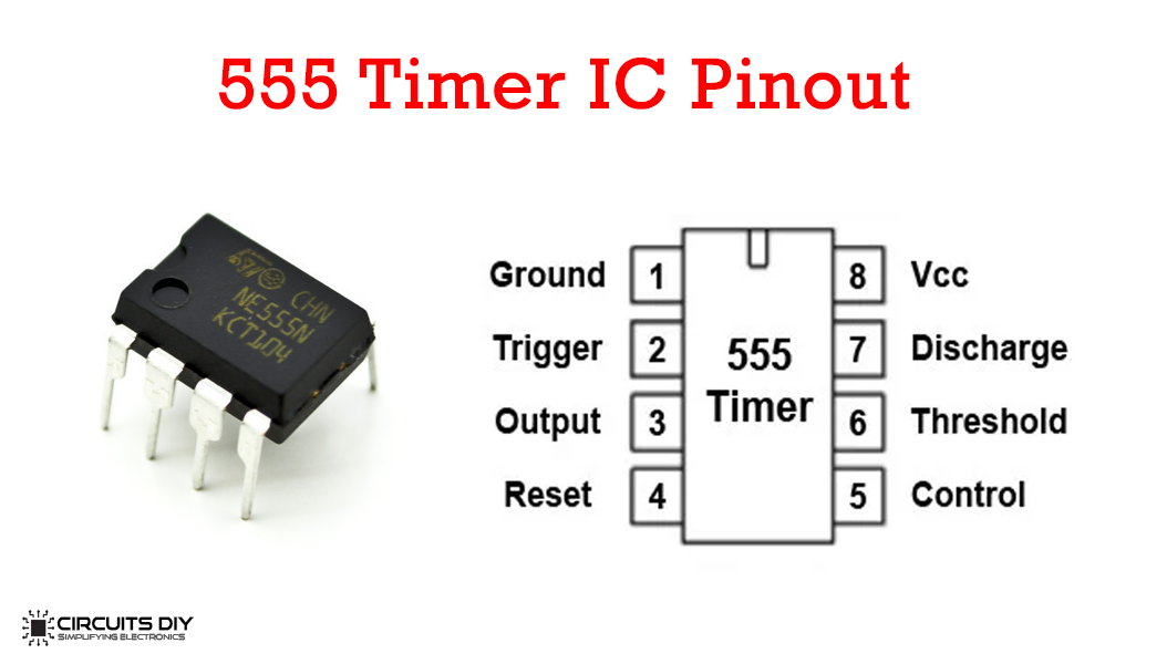
For a detailed description of pinout, dimension features, and specifications download the datasheet of 555 Timer
BC547 Pinout
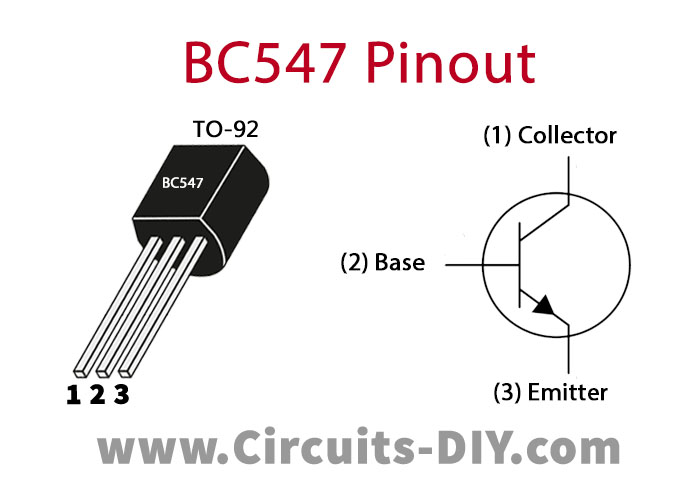
For a detailed description of pinout, dimension features, and specifications download the datasheet of BC547
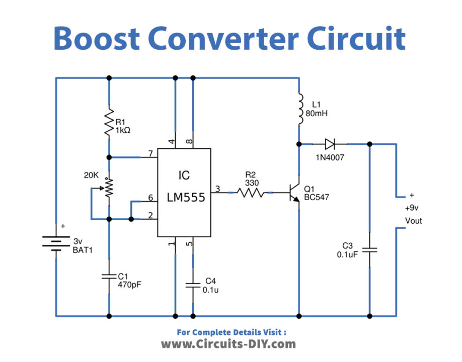
Boost Converter Circuit
Working Explanation
As we can see in the circuit, Timer IC 555 is configured in astable multivibrator mode. The output pulse from the timer IC is applied to the Q1 transistor base, here Q1 acts as a switch, the Collector terminal of Q1 is connected to the positive power supply through inductor L1, and the emitter terminal is connected to the negative supply. IC 555 astable multivibrator mode produces Continuous pulse output, we can increase or decrease the output pulse frequency by changing the value of an RV1 variable resistor. Now the boosted output voltage is taken from the L1 and Q1 meeting point and then Rectified by the diode D1. C3 capacitor removes ripples and noise from the output voltage.
Applications
This DC-DC boost switching converter can be used in telecommunication devices, portable electronic devices, test & measurement devices, and consumer electronic devices.