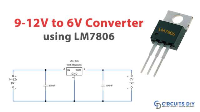
Introduction:
Power converters are commonly used in our daily life at home, commercially, and industrially. Different types of converters are used for different purposes, and they are categorized as AC-AC converters, AC-DC converters, DC-AC converters, and DC-DC converters. All of these have different characteristics and are further divided into subtypes.
A boost converter is one of the simplest types of DC-to-DC converters (also known as choppers) that boost up the voltage at its output. It is classified as a switch-mode power supply that contains two semiconductors (minimum) and at least a single energy storage element. The circuit is simple to build using an inductor, a semiconductor switch, a storage element like a capacitor, and a diode.
This post explains the circuit of a boost converter made using a 555 time IC, a transistor, and a few passive elements.
Hardware Components
The following components are required to make the Boost Converter Circuit
| S.no | Component | Value | Qty |
|---|---|---|---|
| 1. | IC | LM555 | 1 |
| 2. | Transistor | BC547 | 1 |
| 3. | Diode | 1N4007 | 1 |
| 4. | Variable Resistor | 20KΩ | 1 |
| 5. | Resistor | 1KΩ, 330Ω | 1 |
| 6. | Capacitor | 470pF, 0.01µF, 0.1µF | 1 |
| 7. | Inductor | 80µH | 1 |
LM555 IC Pinout
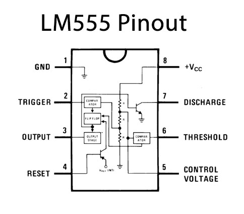
For a detailed description of pinout, dimension features, and specifications download the datasheet of LM555 IC
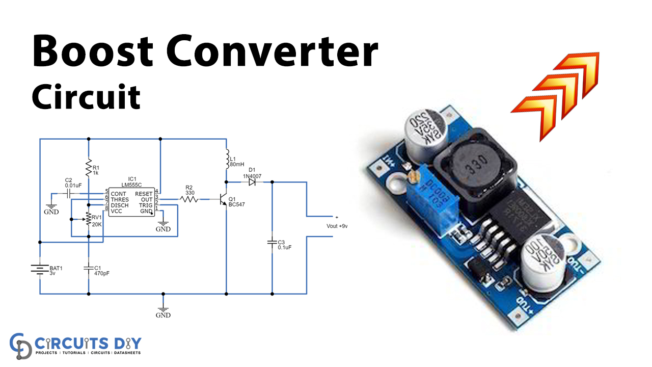
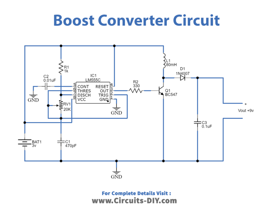
Boost Converter Circuit
Working Explanation
This circuit is designed to provide 9V output voltage using a 3V input source. The time IC 555 is configured in the Astable multivibrator mode that produces uninterrupted output pulse by varying the variable resistor VR1 in order to vary the output pulse frequency. The formula for output frequency and time period is given as:

The transistor BC547 Q1 acts as a switch in the circuit. It receives the output pulse from the 555 IC at its base. The inductor L1 is coupled with the collector terminal of the Q1 and connected to the positive supply while the negative supply is provided to the emitter terminal. The output boosted voltage is acquired at the common point of L1 and Q1 which is then rectified through the diode D1 while the capacitor C3 is used to remove the ripple element from the output signal.
Applications:
The applications of boost converters are as follows:
- It is used in power amplification and battery power systems.
- The circuit is utilized in automotive applications.
- It is also used in communication systems.
Benefits:
The boost converters have low operating duty cycles, provide a high voltage at output derived from the low input voltage and the voltage at MOSFETs is lower.