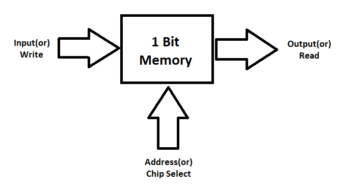
In this tutorial, we are going to make a “ONE bit Memory Circuit”. The memory cell is the fundamental building block of computer memory. If we see the history of computing different memory cell architectures have been used, including core memory and bubble memory. Today, the most common memory cell architecture is MOS memory. Modern random-access memory (RAM) uses MOS field-effect transistors (MOSFETs) as flip-flops. The memory cell is an electronic circuit that stores one bit of binary information. And it must be set to store logic 1 (high voltage level) and reset to store logic 0 (low voltage level). Its value is maintained/stored until it is changed by the set/reset process. The value in the memory cell can be accessed by reading it. If the size of the memory cell increases to greater than one then it must have address lines. And some more memory will have chip select, enable, etc. In digital electronics memory and memory cell circuit plays an important role, every electronic gadget has gigabytes of internal and external memory.
Some schematic utilizes I2C EEPROM or flashes memory ICs. The SRAM (static RAM) memory cell is a type of flip-flop circuit. These require very low power to keep the stored value when not being accessed. A second type, DRAM (dynamic RAM), is based on MOS capacitors. Charging and discharging a capacitor can store a ‘1’ or a ‘0’ in the cell. However, the charge in the capacitor will slowly leak away and must be refreshed periodically. Because of this refresh process, it uses more power. However, greater storage densities can be achieved by DRAM. As we know that one flip-flop can store one-bit status, and more bits can be stored by increasing the number of flip-flops. Here we are going to design and test one bit memory circuit using IC 555.
RS NAND Latch
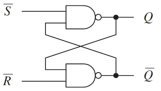
When we need to use static gates as building blocks, the most fundamental latch is the simple SR latch. Where S and R stand for set and reset, it can be constructed from a pair of cross-coupled NOR or NAND logic gates. The stored bit is present on the output marked Q. RS NAND latch example can give a better understanding of one-bit memory cells. The circuit uses feedback to “remember” and retain its logical state even after the controlling input signals have changed. When the S and R inputs are both high, feedback maintains the Q outputs to the previous state. Here when both inputs are given as logic 0 the output goes to undefine (Q, Q’) and if both inputs are given as logic 1 the output remains unchanged. Because the NAND inputs must normally be logic 1 to avoid affecting the latching action, the inputs are considered to be inverted in this circuit (or active low). When S’ or Set pin is given as logic 0 and R’ as logic 1, it will provide output as Q=1 and Q’=0. This is known as the set condition and the output doesn’t change up to return of S’ to logic 1.
Hardware Required
| S.no | Component | Value | Qty |
|---|---|---|---|
| 1 | IC | NE555 Timer | 1 |
| 2 | Resistor | 12KΩ,330Ω | 2,1 |
| 3 | LED | – | 1 |
| 4 | Push-button | – | 2 |
| 5 | Connecting Wires | – | – |
| 6 | Battery | 6V | 1 |
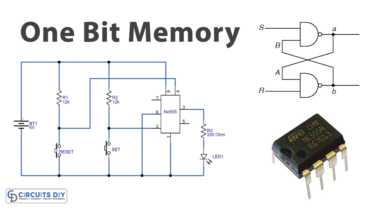
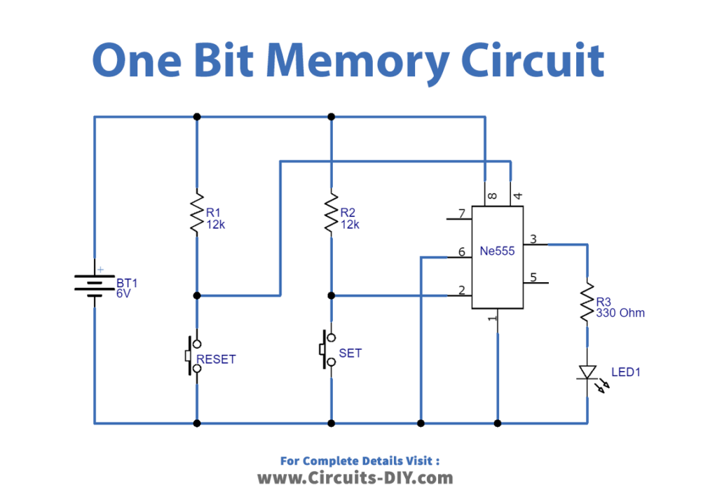
Circuit Diagram
Working Explanation
As we can see in the circuit, IC 555 is used. Here Reset pin and trigger pin are connected to the ground supply through a push-button switch, when the push button is pressed ground supply flow to the corresponding pin. The threshold pin is directly connected to the ground and the output pin is connected to LED to show the stored bit.
Here we powered the circuit. Since the threshold pin is connected to power through a resistor, the output of the internal second comparator of the IC will be low. This low output is fed to the second SET pin of the flip-flop inside the timer. Due to this, the flip-flop will store ZERO in its memory and so the output will be low. As for the low output, the LED will be off.
Now consider the set button is pressed, then the threshold pin is direct gets connected to the ground. Due to this, there will be a higher potential at the positive terminal of the second comparator (inside timer). So the second comparator puts out a positive high signal, and this positive high signal is driven to the flip-flop set pin. So the flip-flop store ONE in its memory and so the Q output will be high. This Q output enables the timer output to go high, so the LED glow to tell ONE is stored in the flip-flop.
One is presently stored in flip-flop memory, now as we press the reset button the PNP transistor inside the timer gets turned on. By this, there will be a high signal MR (Master Reset). This master reset when goes high the flip-flop stored bit gets erased. Due to this, the flip-flop pulls down too low. As the flip-flop goes low the output goes low, and the LED will go off too. This is how a timer stores one bit of data in its flip-flop. If the LED glows, then it represents logic 1. If it is in off condition then it represents logic 0.
Applications
We can use these kinds of memory cells in digital circuits, analog electronic circuits, and hobby circuits we can also use 4-bit or 8-bit memory cells as an electronic lock.