
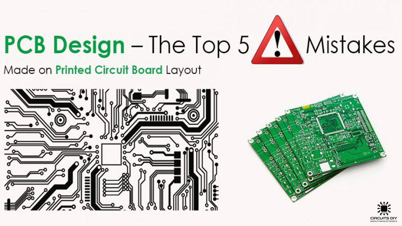
Going about fixing electronics, you tend to learn very soon that fixing & curating electronics is a very hectic process. One of the most intricate & complex devices among them is the Printed Circuit Board or PCB for short. PCB designing is a process in which even the most common mistakes are bound to occur. What are those mistakes? How do we avoid them?. In this article, we will be focusing on the most common PCB design mistakes that occur in our day to day design process & how can you start to avoid them today.
Whether you choose to do the PCB design yourself or hire an engineer, PCB design errors happen every now & then. But by properly debugging the following mistakes you can take you PCB design skills to the next level.
Common Mistakes In PCB Designing
1) Incorrectly Locating Decoupling Capacitors
Decoupling capacitors always connect in parallel with the power supply in order to supply a stable voltage to critical PCB components. Decoupling capacitors need to be as close as possible to the pin that needs the stable voltage to be effective. The power line coming from the power source should be route properly so it goes to the decoupling capacitor before going to the pin needing a stable voltage.
2) Fault In Landing Patterns
Almost every PCB CAD software includes libraries of components. These libraries include the schematic symbol and PCB landing pattern for each component, as long as you stick with theses libraries you shouldn’t run into any sort of issue. But, if you use a part outside of these libraries then you have to draw the circuit symbol and the PCB landing pattern by hand. It’s easy to make mistakes, especially on the landing pattern. For instance, if the pad to pad spacing is off by as little as a fraction of a mm, the pins won’t align properly making soldering impossible.
3) Incorrect Antenna Layout
When dealing with PCBs of wireless devices/products, the PCB layout of the antenna is very critical. Proper impedance matching is very important to ensure max power transfer between the transceiver and the antenna. This requires two things, first is a microstrip of correct impedance (50 Ohm) connecting the antenna and the transceiver. In addition to that, it is also important to add an LC matching network such as a π – network.
4) Insufficient Width of High Power Traces
The minimum PCB trace width threshold won’t be sufficient if the PCB Board traces has to house currents greater than 500mA. A trace on an outer layer can carry more than an internal trace for the same thickness. This is because the external trace has superior airflow and thermal dissipation. The width depends on how much copper is being used for that layer. Most PCB manufacturers allow you to choose from various copper weights from 0.5 oz/sq.ft to 2.5 oz/sq.ft.
5) Inefficient Layout Of Switching Regulators
Most designers tend to prefer linear voltage regulators over switching regulator due to its cost. But, even though linear regulators are easier to layout on PCBs, they can waste a lot of power. On the other hand, Switching regulators are more complex, but much more efficient. However, they require to be more carefully layout on the PCB, so the datasheet guidelines must be followed closely.
So by avoiding the above mistakes you can step up your PCB design skills to the next level.
Related posts:
 Wave Soldering Process In PCB Assembly | Everything You Need To Know
 Key Environmental Factors To Manage During SMT Manufacturing
 Chemical Used in the Etching Process of Printed Circuit Board(PCB)
 Saving Time And Money In PCB Manufacturing | Five Golden Rules
 Crafting Uniqueness: A Guide to Custom PCB Assembly
 Standard Thickness of the Printed Circuit Board(PCB)


