
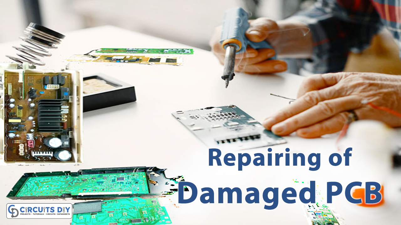
Introduction
Are you in trouble that your Printed circuit board gets wasted when a problem or error occurs? Do you think that it gets expired after some time? And this all wastes a lot of your money. But, did you know that you can repair PCB by yourself by following several steps? And once you understand this skill, you will be able to repair simple as well as difficult circuits. So, in this article, we are going to learn about how to repair PCB.
Tools Needed to Repair PCB
To perform repair there are some necessary tools required
- Soldering Iron
- knife
- Desoldering equipment
- Multimeter
- Copper tape
- PCB Holder
Steps to Repair PCB
To repair your PCB or restore the damaged track, component, or element, you need to follow some major steps. Remember, to be cautious while repairing. If you follow these steps, you can handily repair any PCB. The steps are given below.
1) Remove the damaged element or track
Step one is to remove the damaged track or element. But first, secure the PCB using its holder. You can also use tape for this purpose. After that, using a multimeter check continuity or analyze the circuit. Diagnose where the problem is. Once you are done with it, through the desoldering equipment, remove that part. However, for SMT components you need a hot air blower to remove the element.
2) Clean the track of the PCB
Once you get done removing the track. Now it’s time to clean It. Use a sharp knife or a screwdriver to remove the still-existing solder. Ensure that the exposed element or track must be clean
3) Place a Copper Tape
Over that cleaned and exposed track, place copper tape on an area of PCB where you’re working. The tape should overlap the existing component or track.
4) Solder the Tape Joints
Now, it’s time to join the solder joints. But, remember that copper tape melts instantly. Use limited heat. Carefully, solder the joints where the new copper joins.
5) Make a Whole and Solder the component
Rub the area to push down copper tape over the pad area. Pierce, to make a through-hole. Now, solder the new component. Use the normal method to fit and solder the required element or component. Since the new pads are sensitive, so try to use the heat as low as possible for soldering.
6) Trim the excessive Copper
Using a knife, or scissors, trim, or remove the excessive copper carefully. Clean or wipe out that copper. Now, your repaired PCB is ready to use. Check the circuit and use it for your device.
Conclusion
We, designers or students, invest a lot of time and a bunch of money to make circuits and devices. But it affects us when things get worse or get expired. And therefore, it is necessary to utilize some more time on repairing rather than making new. Repairing saves money and time. Moreover, it also allows redeeming the circuits. Nothing is garbage until we make it.
Related posts:
 Wave Soldering Process In PCB Assembly | Everything You Need To Know
 10+ Best Free PCB Design Software
 Multi-Layer PCB Applications & Advantages
 SMT PCB Assembly Process - A Complete Guide For Beginners
 Top 7 PCB Layout Design Tips & Best Practices For Beginners
 PCB Material for High-Frequency Applications


