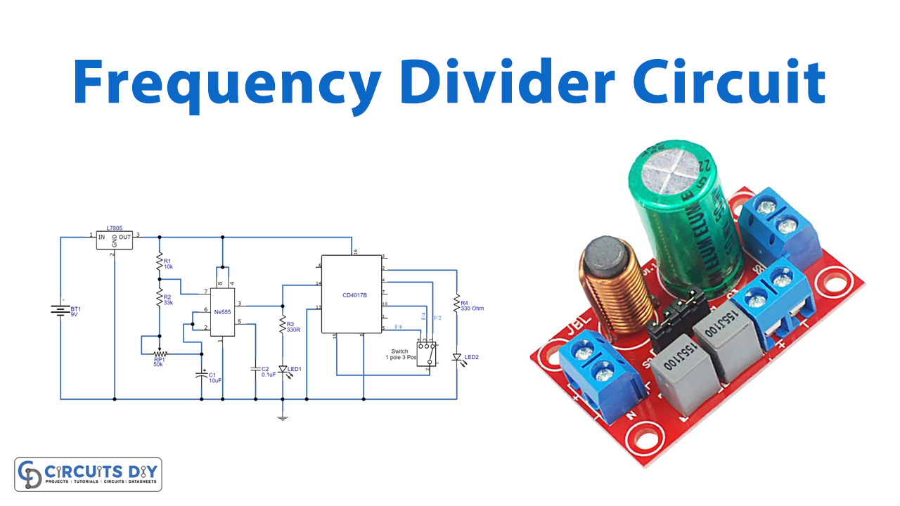
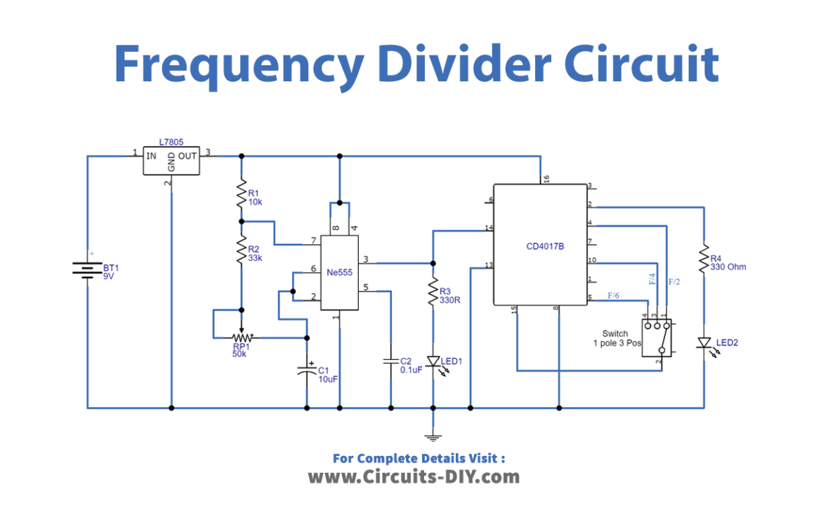
In this tutorial, we are going to make a “Frequency Divider Circuit”.
Sometimes we came across a situation where we have only one source of signal with a specific frequency and need to obtain the signal of several frequencies. For example, when we are working with digital logic circuits and some analog multiplex circuits. In this kind of situation, we need frequency divider circuits. And making a perfect frequency divider is quite difficult, here we design a simple frequency divider circuit by using timer IC 555 and decade counter IC CD4017. The CD4017 IC counts from 0 to 10 hence the name decade, it is not a standard ring counter, meaning it does not trigger all flip flops at the same time. Therefore, it uses the Johnson counter technique to achieve flip flop count. We know frequency dividers make any input frequency f divided by n integer value (f / n), the following circuit takes input frequency f and gives output frequency as (f / 2), (f / 4), and (f / 6). Here timer IC 555 which acted as an astable multivibrator used to generate square pulse signal and it can be tuned to different frequencies by a variable resistor. This divided frequency output is taken from the decade counter Q1 pin.
Hardware Required
| S.no | Component | Value | Qty |
|---|---|---|---|
| 1. | Decade Counter Divider IC | CD4017 | 1 |
| 2. | IC | NE555 Timer | 1 |
| 3. | Regulator IC | LM7805 | 1 |
| 4. | Variable Resistor | 50KΩ | 1 |
| 5. | Resistor | 10KΩ, 33KΩ, 330Ω | 1, 1, 2 |
| 6. | Capacitor | 10uF, 0.1uF | 1, 1 |
| 7. | LED | – | 2 |
| 8. | Switch 1 pos, 3 pos | – | 1 |
| 9. | Switch | – | – |
| 10. | Battery | 9V | 1 |
Circuit Diagram
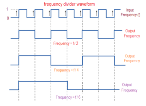
Output Waveform
Working Explanation
As we can see this frequency divider circuit has two stages one is the input frequency generator and another one is the decade counter/divider. Here IC 555 is configured as an astable multivibrator, timing resistor R1, R2, and variable resistor VR1 are connected with timing capacitor C1, discharge pin7 is connected between R1 and R2 then threshold pin6 and trigger pin2 are connected between VR1 and C1. Then 5V Vcc is applied to the bias pin8 and reset pin4. And control voltage pin5 is connected to the ground through a 0.1 uF C2 capacitor. Output pin 3 is connected with the clock pin of decade counter IC and LED1, this LED indicates the frequency of the input signal.
Here 4017 Counter IC is responsible for dividing the frequency by f/2, f/4, or f/6. An SPDT switch is used for selecting frequency. IC 4017 takes the input clock at pin 14 and provides decade output from Q0 to Q9. To convert this into a frequency divider we have taken the output from Pin 2 and connected it with LED2 through R4, this will visually indicate the output frequency through blinking (LED D1 will blink with frequency f, and LED D2 will blink with frequency f/2 or f/4 depending upon the position of SPDT switch). Active low enables pin 13 to be grounded and Reset pin 15 to be connected with a three-way switch towards Q2 for F/2 output selection (the counter IC can reset itself and starts from the beginning (Q0). This means for the first clock pulse output Q1 will be high and for the second clock pulse output, Q2 will be high which resets the IC and makes the output Q0 high. For the third clock pulse output, Q1 will be high again and the LED will glow. So, for every two-input clock pulse, LED D2 will be high once, that is how it divides the frequency by 2), Q4 for F/4 output selection (in this IC 4017 will be reset in the 4th pulse), and Q6 for F/6 output selection (in this IC 4017 will be reset in the 6th pulse). A LED D2 is connected to pin 2 of IC 4017 through a 330-ohm resistor, which indicates the divided frequency. And a 7805 IC is used to regulate the voltage.
Finally, when we have connected a 9v Battery to power the circuit, and connect an oscilloscope at output pin 2 we can obtain a divided output frequency. Here the first signal represents input frequency (f) and output frequency (f/2), (f/4), and (f/6) are shows the divided frequency results.
Applications
Can be used in digital logic circuits and some analog multiplex circuits.