
Introduction
In electronics, an adder is a digital logic circuit that is commonly used to add integers. We use adders in many systems and other types of processors to calculate addresses and associated actions, as well as construct table indices in the ALU and other portions of the CPU. We classify these adders into two different types; half adder and full adder. Here in this tutorial, we are going to the “Full Adder Circuit Diagram”
In one of our articles, we have already discussed the half adder. A half-adder differs from a full-adder in that the full-adder has three inputs and two outputs, while the half-adder has just two inputs and two outputs. The first two inputs are A and B, with the third being a C-IN input.
Brief Overview of Full Adder
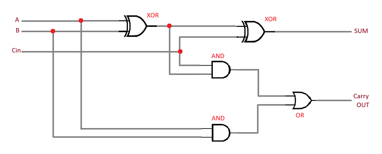
Most digital circuits that perform addition or subtraction use a full adder circuit. It gets its name from the fact that it adds two binary digits plus a carry-in digit to generate a total and carry-out digit. It has three inputs and two outputs. Input includes A, B, and Cin; while outputs are Sum and carry calculated as:
- Sum = A⊕B⊕Cin
- Carry out = A.B + (A⊕B).Cin
Truth Table for Full Adder
| A | B | Cin | Sum | Cout |
|---|---|---|---|---|
| 0 | 0 | 0 | 0 | 0 |
| 0 | 0 | 1 | 1 | 0 |
| 0 | 1 | 0 | 1 | 0 |
| 0 | 1 | 1 | 0 | 1 |
| 1 | 0 | 0 | 1 | 0 |
| 1 | 0 | 1 | 0 | 1 |
| 1 | 1 | 0 | 0 | 1 |
| 1 | 1 | 1 | 1 | 1 |
The resulting sum is an addition operation between A, B, and Cin, while the resulting carry is an OR logic operation between A.B and Cin.
Hardware Required
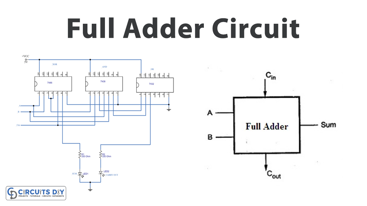
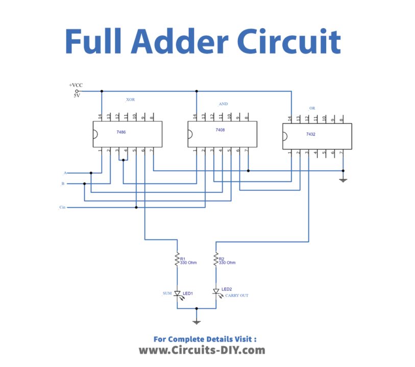
Circuit Diagram
Working Explanation
We built the full adder circuit using XOR gate IC 7486, logic AND gate IC 7408, and OR gate IC 7432, all of which are quad 2 input logic gate ICs. Wire Vcc and GND to the logic IC, then connect Input A, and B to the first XOR gate input which is pin 1 and, the output of the first XOR gate is coming at its pin 3 and is going to the next XOR gate input which is pin 4, The third input Cin is going to XOR gate input pin 5. A⊕B, Cin is the input to the second AND gate.
Sum Result is collected from XOR gate pin 6 and linked to LED1 via R1. OR gate adds two AND gate outputs, then OR gate pin 3 is used as the Carrying out output and linked to LED2 through the R2 resistor. Verify the whole adder truth table after you’ve made the connection. When an LED light glows, it indicates logic High, whereas when it is turned off, it represents logic Low.
Application and Uses
- The Arithmetic Logic Unit (ALU) uses Full Adders to generate memory locations within a computer.
- For graphics-related applications, full-adders are a component of the Graphics Processing Unit.
- Used in the ripple carry adder circuits, etc.