Introduction
In electronics, an adder is a digital logic circuit that is commonly used to add integers. Adders are used in many systems and other types of processors to calculate addresses and associated actions, as well as construct table indices in the ALU and other portions of the CPU. These adders are classified into two different types; half adder and full adder. Here in this tutorial, we are going to discuss the “Half Adder Circuit Diagram”
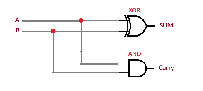
Half adders are a sort of adder, which is a circuit that adds numbers. The half adder can add two single binary numbers and output the result along with the carrying value. It has two inputs; A and B inputs and two outputs; sum and carry
Brief Overview of Half Adder
A half adder adds two single-digit binary integers together to produce a two-digit output. To put it another way, it only does half of the job of a complete adder. The half adder accepts two inputs. If the inputs are A and B, the outputs will be Sum and Carry. Whereas;
- Sum = A ⊕ B
- Carry = A . B
Here, Sum is an addition between A and B, while Carry is an AND logic operation between A and B.
Half Adder Truth Table
| A | B | A + B | Binary Output | Sum (A ⊕ B) | Carry (A ⋅ B) |
| 0 | 0 | 0 + 0 | 0 | 0 | 0 |
| 0 | 1 | 0 + 1 | 1 | 1 | 0 |
| 1 | 0 | 1 + 0 | 1 | 1 | 0 |
| 1 | 1 | 1 + 1 | 10 | 0 | 1 |
We can observe from the truth table above that the sum digit of two binary inputs results from an XOR operation, which we can do using an XOR gate. The result of the AND operation is the carry digit of those two binary inputs, which we may achieve using an AND gate.
Hardware Required
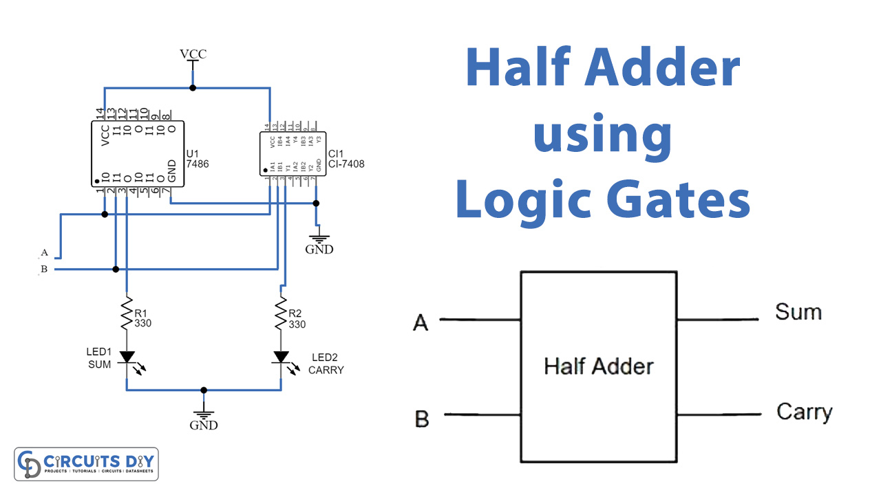
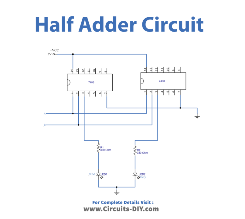
Circuit Diagram
Working Explanation
We built this half adder circuit using XOR gate IC 7486 and Logic AND gate IC 7408, both quad 2 input logic gate ICs. Wire Vcc +5V and GND to logic IC, then connect input points A, B to the XOR gate input and then the AND gate input. Both ICs provide an output at pin 3, therefore the XOR gate output is wired to the LED1 using the R1 resistor which indicates the Sum output. We link the LED2 to the AND gate output through the R2 resistor which shows the Carry output. When the LED lights up, it reflects high logic. If the LED remains turned off, it signals logic LOW.
Application and Uses
- Utilized in arithmetic logic units of computers or processors.
- Also, to make full adders.
- Calculators, etc