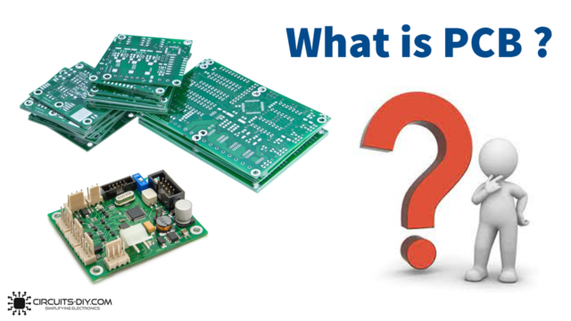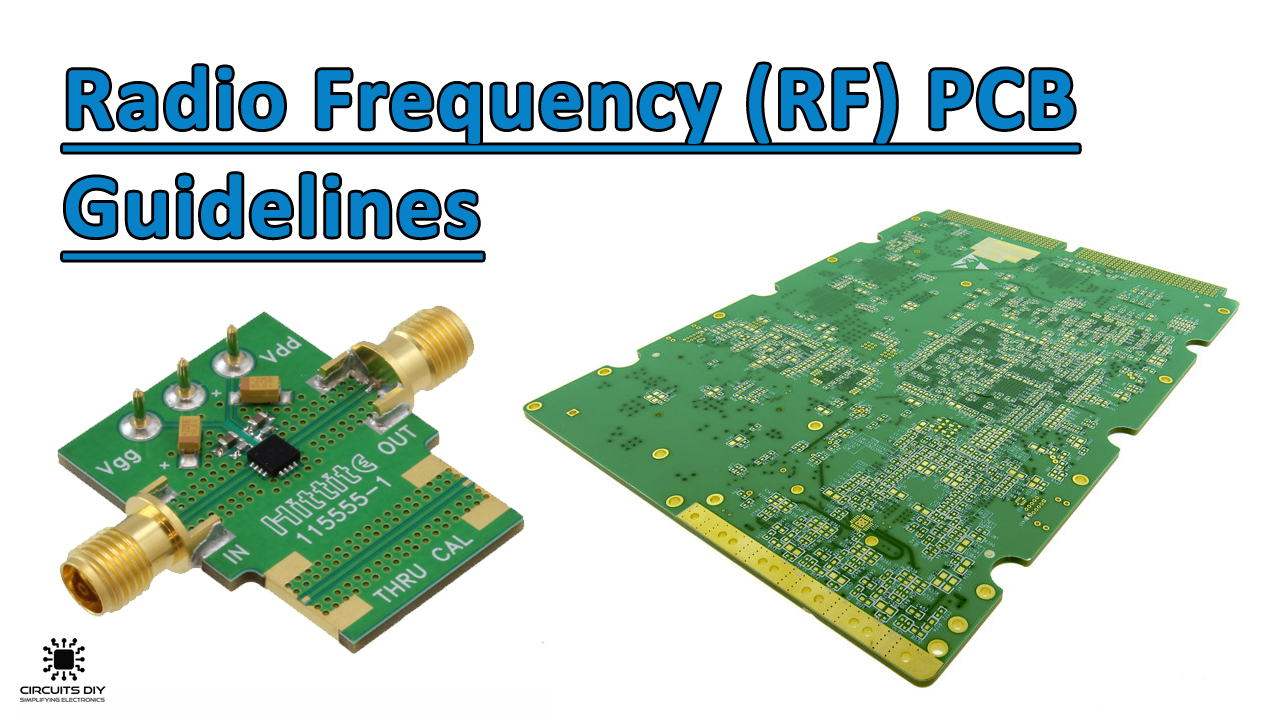
Radiofrequency printed circuit sheets (RF PCBs) are an interesting, fast-developing segment of the PCB producing industry. The PCB market considers an RF circuit board to be any high-frequency PCB that works above 100MHz. This article gives guidelines to an RF printed circuit board (PCB) layout and format. The article content design in such a way to give you the best possible practice guidelines from its basic layers to final layout considerations. All the specific electronic devices use to develop by relevant design and assembling rules.
RF Transmission Lines
A large number of Maxim’s RF segments require controlled impedance transmission lines that will move RF capacity to (or from) IC pins to the PCB. These transmission lines can actualize on an outside layer (top or base), or covered in an interior layer. Rules for these transmission lines incorporate discussions associating with the coplanar waveguide, suspended stripline, microstrip, and trademark impedance.
Ground Planes
It must not be broken under transmission line steering. Ground vias between layers ought to include generously all through the RF segment of the PCB. This forestalls the accrual of parasitic ground inductance because of ground-current bring ways back. The vias likewise help to keep cross-coupling from RF and other signal lines over the PCB.
Bias and Ground Layers
The layers dole out to the systematic bias and ground must consider as far as the return current for the segments. The general guidance is to not have signals steered on layers between the ground layer and the bias layer. In the figure, it is shown that there are no layers between the “bias and ground return layer”

Signal Line Isolation
You have must care to forestall unintended coupling between signal lines.
Grounding of Shunt-Connected Components
For shunt-connected grounded parts, for example, power-supply decoupling capacitors, the prescribed practice is to use at any rate two establishing vias for every segment. This lessens the impact of through parasitic inductance.

IC Ground Plane
Some ICs require a solid ground plane on the segment layer (top or base of PCB) straightforwardly beneath the segment. However, this ground plane will bring DC and RF return flows through the PCB to the doled-out ground plane. The auxiliary capacity of this segment ground paddle is to give a thermal heatsink, so the paddle ought to incorporate the most extreme number of through vias that permit by the PCB configuration rules. The figure presents a 5 × 5 array of via holes. This array of holes is embedding in a “central ground plane” directly under the Radiofrequency IC.

Selection of Decoupling or Bypass Capacitors
Capacitors have restricted successful frequency extends because of their self-resonant frequency (SRF). The SRF is accessible from the producer. But some time must describe by direct measurement. Over the SRF, the capacitor is inductive and thusly won’t perform the decoupling or bypass function. At the point when it requires broadband decoupling, standard practice is to utilize a few capacitors of expanding the size of capacitance, all connections in parallel.
Power Routing and Supply Decoupling
A typical practice is to utilize a star arrangement for the power supply routes if a segment has a few supplies connections. A more considerable decoupling capacitor is mount at the root of the star, and less considerable capacitors at each of the star branches. The estimation of these last capacitors relies upon the working frequency range of the RF IC, and their particular functionality.
Bypass Capacitor Layout
Since the supply lines must be AC ground, it is critical to limit the parasitic inductance add to the AC ground return path. These parasitic inductances can be brought about by design or component orientation arrangements. For example, the direction of a decoupling capacitor’s ground. This figure shows the least total footprint for the “related vias” and “bypass capacitor”