In this tutorial, we are going to make a “Simple IC 555 Voltage Doubler Schematic”.
When we need to charge a pump, DC to DC boost converter, and if our design includes a stepper motor or servo motors we can simply generate bias for those motors from this simple voltage doubler circuit. We don’t need a separate power supply circuit. A voltage doubler is a circuit that gives an output voltage double of applied at its input. These circuits use capacitors to store energy and are in some form rectifier circuits. The switching components are generally diodes, which help to bring down the cost instead of using a more expensive counterpart for example a MOSFET, or a BJT. Here we construct a simple and easy IC 555-based voltage doubler circuit. This will double the Input bias from 5V – 9V to 10V – 18V and delivers high-frequency square pulse output. This circuit doesn’t have any over-current draw protection setup and the load current output is slightly unstable so it is suitable for low current applications only.
Hardware Required
| S.no | Component | Value | Qty |
|---|---|---|---|
| 1. | IC | LM555 | 1 |
| 2. | Capacitors | 33μF/50V, 0.01μF | 2, 2 |
| 3. | Diode | 1N4007 | 2 |
| 4. | Resistor | 8.2KΩ, 30KΩ | 1, 1 |
| 5. | Connecting Wires | – | 1 |
| 6. | Battery | 5V-9V | 1 |
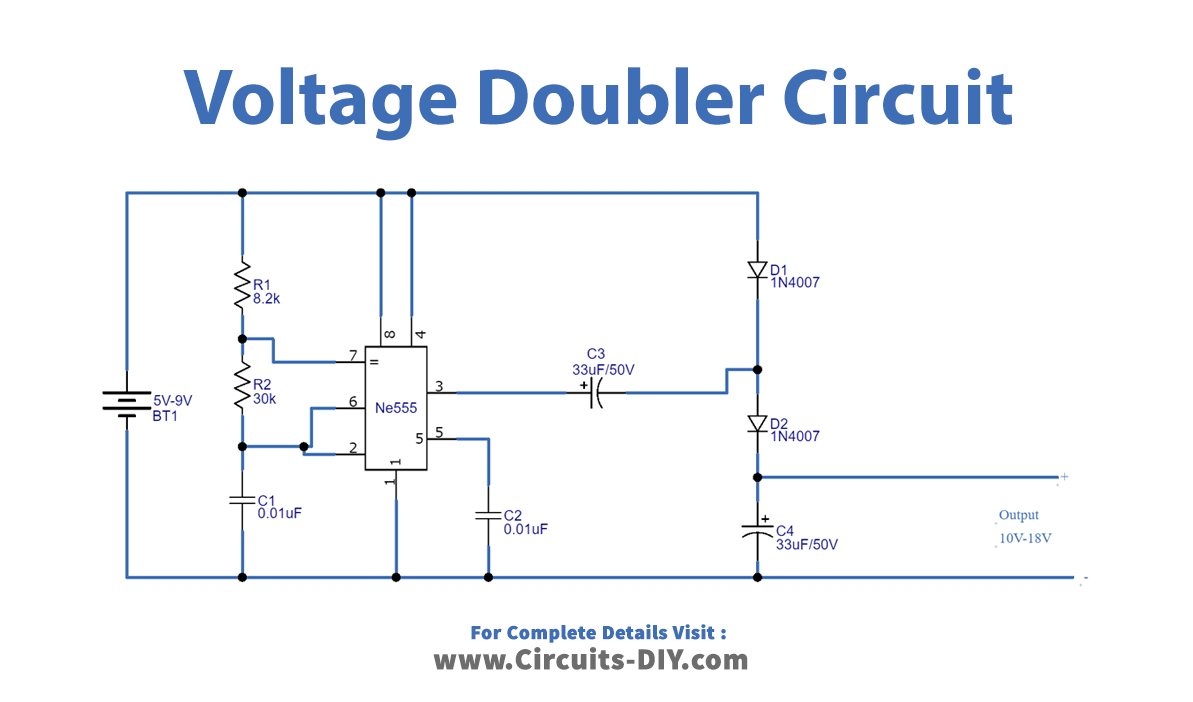
Circuit Diagram
Working Explanation
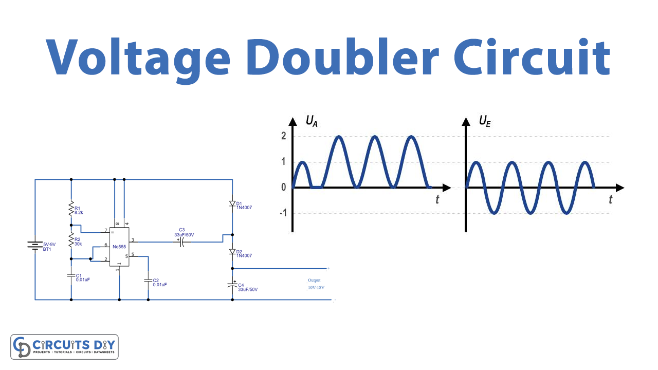
As we can see the circuit consists of an astable multivibrator circuit that generates a square wave at the output terminal 3, with a 50% duty cycle. The capacitors C3 and C4 charge alternately with the ON and OFF states of the output. When the output is low the capacitor C3 charges and at a high state capacitor C4 charges. This circuit delivers high-frequency square pulse output and the C3 capacitor holds the pulse charge, the D2 diode rectifies the positive peak of square pulse and C4 gets the peak voltage charge and gives doubled output voltage combined with input bias through the D1 diode. Diode D1 and D2 also prevent the discharging of the capacitors. The applied input voltage should be at the limit of IC NE555 operating voltage. If the input voltage is 1V then the output voltage taken across the capacitors will be 2V, which is double the supply voltage.
This circuit will provide output duration depending on timing resistor R1, R2, and timing capacitor C1.
Period = TH + TL = 0.693 (R2 + 2 R1) C1
Frequency = 1.44 / (R2 + 2 R1) C1
We can obtain a different level of output by changing these timing components, but very low frequency or very high-frequency output from a timer won’t give the best output voltage.
Applications
They serve in many electrical and electronic applications such as in microwave ovens, strong electric field coils for cathode-ray tubes, electrostatic and high voltage test equipment, etc.