In this tutorial, we are going to make a “Full Adder Circuit”. In our day-to-day activities, we use cell phones, PDAs, and many more. These are digital electronic devices, that comprise comparators, dividers, Adders, etc. The functionality and performance of digital electronic devices mainly depend on how efficiently these basic circuits operate. Here the adder is a digital circuit used to perform addition on binary numbers. The adders are used to perform the Arithmetic Logic Unit (ALU) task in the processors when it comes to the computers. In processors, they are used to calculate addresses, increment or decrement operations, table indices, and other operations.
We are going to design a full adder circuit diagram, which adds three binary bits and gives the result as S Carryout out. It can be used in many applications like Encoder, Decoder, BCD system, Binary calculation, address coder, etc.., the basic binary adder circuit is classified into two categories are
- Half Adder
- Full Adder
Full Adder
When the addition of two binary digits is performed, then the sum is generated. If it consists of two digits in the output then the MSB bit is referred to as carrying. This is treated as the third bit in the process of addition. The ‘combinational circuit’ which is capable of performing addition on three input bits that is two inputs and the carry-in from the previous operation is known as Full Adder. Here three input and two output Full adder circuit diagrams are explained with logic gates circuit and also logic IC Circuits.
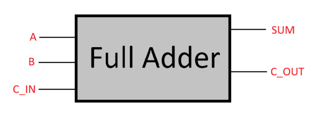
The full adder will take three inputs named A, B (two standard inputs), and Cin (Carry C) then it will give two outputs named Sum, and Carryout. The full adder inputs are three, and they are the A, B, the, and the Carry C.
Sum = A ⊕ B ⊕ Cin
Carry out = A.B + (A⊕B). Cin
The resulting sum is exclusively an addition between A, B, and Cin the results carry is OR logic operation between A.B then A⊕B, and Cin. From the above equation of the sum, it is easily visible that first A and B are XORed together, then Cin. ⊕ is the symbol of the XOR operation. In the Carry out expression, we can see that first A and B are ANDed together, and then the Cin is ANDed with the XORed for A and B. Then, these results are ORed together to produce the Carry out the equation.
Full Adder Logic Gate Diagram
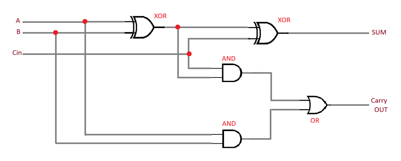
Two input XOR gate, two-input, AND gate, and two-input OR gate form the full adder logic circuit, Input & Output of this logic diagram can be derived by the following truth table.
Full Adder Truth Table
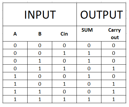
In the full adder, the first carry C is always zero when the first add operation starts. When the Sum S is generated from A and B, the carry from the last least significant bit is added to the next to add operation, and this task is continued till all the binary numbers are added. The full adder also can add 8, 16, 32, etc. bits binary numbers, which is why it is the component in the cascade of adders. The full adder usually produces a two-bit binary number as the output. When both inputs are low then the sum and carry out will be logic low (0), if anyone’s input is high then the sum will be logic high (1), and carry out will be logic low (0), when two inputs are high then sum becomes logic low (0) and carry out becomes logic high (1) when all inputs are high (1) the output sum and carry out will be logic high (1).
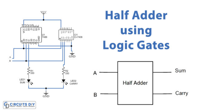
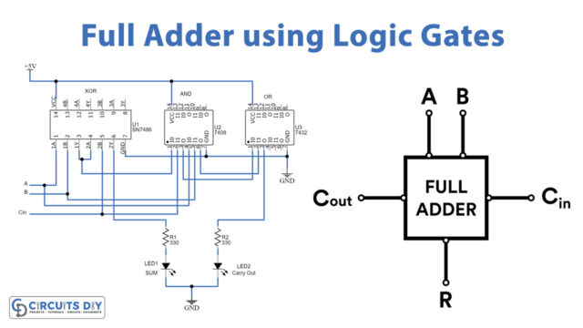
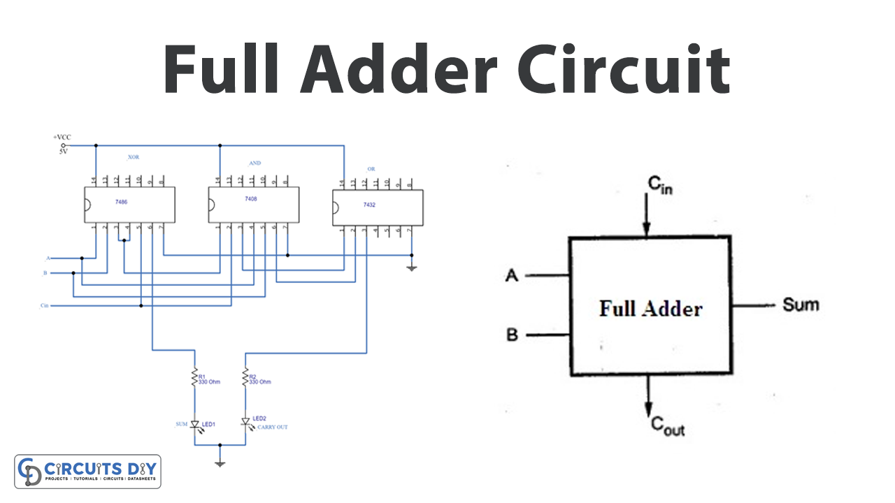
Hardware Required
| S.no | Component | Value | Qty |
|---|---|---|---|
| 1. | IC | 7486, 7408, 7432 | 1, 1, 1 |
| 2. | Resistor | 330Ω | 2 |
| 3. | LED | – | 2 |
| 4. | Battery | 5V | 1 |
| 5. | Connecting Wires | – | – |
Full Adder Circuit

Working Explanation
As shown in the circuit, we construct the full adder with IC 7486 (XOR gate) and IC 7408 (AND gate), and IC 7432 (OR gate), all are quad 2 input logic gates ICs. First, connect Vcc +5V and GND supply to us. Here input A, and B is connected to the XOR gate input then AND gate input, the output of the first XOR gate (Pin 3) is connected to the next XOR gate input pin 4, and Cin is connected to the XOR gate input pin 5. Second AND gate take A⊕B, and Cin as inputs. XOR gate pin 6 taken as Sum Result and connected to LED1 through R1. Two AND gate outputs are added by OR gate then OR gate pin 3 is taken as carrying out output and connected to LED2 through R2 resistor. Finally, now we have to verify the full adder truth table. When LED glows it represents logic High (1), during the OFF condition LED represents logic Low (0).
Applications
The full adders are used to program the chips, and these chips are used in modern vehicles, planes, and other automatic machinery.